Technology
Toshiba Announces Gallium Nitride Power FET with World's Highest Output Power in Ku-band

Achievement of 65.4W Output Power at 14.5GHz
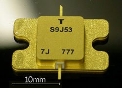
TOKYO - Toshiba Corporation today announced that it has developed a gallium nitride (GaN) power field effect transistor (FET) for the Ku-band (12GHz to 18GHz) frequency range that achieves an output power of 65.4W at 14.5GHz, the highest level of performance yet reported at this frequency band. The main application of the new transistor will be in base stations for satellite microwave communications, which carry high-capacity signals, including high-definition broadcasts. Toshiba plans to start sample shipment of the new power FET by the end of 2007 and to go into mass production by the end of March 2008.
Advances in Ku-band microwave amplifiers focus on replacing the electron tubes conventionally used at this bandwidth with semiconductors, particularly GaN devices, which offer advantageous high power characteristics at higher microwave frequencies.
The new power FET has a high electron mobility transistor (HEMT) structure that Toshiba has optimized for the Ku-band. The company replaced source wire bonding with via hole technology*1 to reduce parasitic inductance, and also improved overall design of the matching circuit for practical application at Ku-band frequencies.
Demand for GaN power FET for radars and satellite microwave communications base stations is growing steadily, both for new equipment and replacement of electron tubes. Toshiba will meet this demand with early commercialization of its new Ku-band power FET.
Full details of the new GaN power FET will be presented at the European Microwave Conference 2007, in Munich, Germany from October 8 to 12.
Background and development aims
Ever increasing communications flows in satellite microwave communications are driving demand for higher output power in signal amplifying devices, as is development of more powerful radar systems. Demand is particularly strong for GaN devices, which offer advantages over conventional gallium arsenide devices in heat dissipation and high power performance characteristics at high frequency.
Toshiba has taken the lead in applying GaN technology to power FET for microwave frequency applications. The company directed its initial efforts to the development and marketing of power FET for the 6GHz band (2005) and 9.5GHz (2006) band, and developed devices that achieved the worlds highest output power at those frequencies. The company has now extended its line-up to 14.5GHz. Toshiba will continue development for the18GHz to 30GHz frequencies (Ka-band) and beyond.
Outline of development
-
1. Device technology
Toshiba achieved the outstanding performance of the new FET by optimizing the composition and thickness of the AlGaN and GaN layers formed on the highly heat-conductive silicon carbide (SiC) substrate of the HEMT structure. To assure high performance at Ku-band frequencies, Toshiba has applied a shorter gate length of below 0.3 microns, and optimized the shape of each electrode and element configuration to enhance heat dissipation.
-
2. Process technology
To reduce the parasitic inductance and improve higher frequency performance, Toshiba developed a unique technology for forming via holes, which pass from the surface source electrode through the chip to the ground. Success in forming via holes in SiC substrate, recognized as a highly demanding process, is a breakthrough in development of the new FET.
As gate lengths shorten, suppression of current leakage at the gate electrode is essential for achieving high level performance. A unique overcoat process applied around each gate electrode contributes to suppressing gate leakage to 1/30 that of Toshiba's conventional approaches. Electron beam exposure technology is applied in order to secure stable processing of gate lengths below 0.3 micron meters.
Key characteristics
This table can be scrolled horizontally.
| Linear gain | 8.2dB |
|---|---|
| Saturation power | 65.4W |
| Drain voltage | 30V |
| Operating frequency | 14.5GHz |
| Chip size | 3.4mm x 0.53mm |
| Package size | 21.0mm x 12.9mm (external dimension) |
October 09, 2007


