
- Media data analysis
Deep learning defect inspection
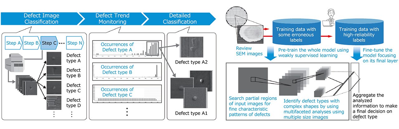
Accurately decide the presence and type of defects based on inspection images.
- Toshiba achieved highly accurate defect detection by combining a deep learning model that distinguishes complex shapes with weakly supervised learning that is resistant to label noise.
- Used in the Toshiba Group’s semiconductor manufacturing facilities.
Applications
- Image inspection at manufacturing sites
Benchmarks, strengths, and track record
- International Symposium on Semiconductor Manufacturing (ISSM) 2018 Best Paper Award
- Japanese Society for Artificial Intelligence (JSAI) 2016 Field Innovation Award; Gold Prize
- Used at Toshiba Group manufacturing bases.
Inquiries
Please include the title “Toshiba AI Technology Catalog: Deep learning defect detection” or the URL in the inquiry text.
Please note that because this technology is currently the subject of R&D activities, immediate responses to inquiries may not be possible.
References:
- K. Imoto, et al., “A CNN-Based Transfer Learning Method for Defect Classification in Semiconductor Manufacturing,” IEEE Trans. on Semiconductor Manufacturing, vol. 32, no. 4, pp. 455-459, Nov. 2019.
- Kazunori Imoto et.al., “Automated Defect Classification System for Semiconductor Manufacturing Processes Using Deep Learning”; Toshiba review, Vol. 74, No. 5, 2019. (PDF)
- Japanese Society for Artificial Intelligence (JSAI) 2016 Field Innovation Award; Gold Prize: Semiconductor productivity improvements at the Yokkaichi Operations
- The world’s leading semiconductor manufacturing processes, supported by AI (Toshiba Digital Solutions Corporation)
- Toshiba Review; Vol.72, No.1, p.36 (March 2017) (PDF) (in Japanese)
