![]()
Toshiba's industrial artificial intelligence (AI) technologies have culminated in Toshiba's "SATLYS" analytics AI. The advanced case examples of the Toshiba Memory Corporation's Yokkaichi Operations represent the best this AI has to offer. The market's demands for NAND flash memory are strict, calling for high capacities and low prices. In order to meet these demands, the plant, which had been actively making bold investments in facilities and development, began implementing AI-based semiconductor manufacturing process innovations. They fused the cutting-edge technologies of Toshiba's Corporate Research & Development Center, the extensive manufacturing and system integration experience, know-how, and broad-ranging operation knowledge of Toshiba Digital Solutions Corporation, and the on-site knowledge of Toshiba Memory Corporation, an expert in site operation. Manufacturing site operations were supported using high accuracy yield analysis and defect inspection. They produced manufacturing processes unparalleled anywhere in the world, both improving quality and management levels and streamlining production processes. Let's look at the "ultra-smart plant" achieved through the use of Toshiba AI.
Visualization of two billion items per day of big data
The Toshiba Memory Corporation Yokkaichi Operations, located in Mie Prefecture, is one of the world's top NAND flash memory production sites that is roughly ten times the size of the Tokyo Dome. This largest plant in Japan has four our clean room buildings, are home to over 5,000 machines, spanning 200 types. Each clean room is connected by conveyor belts in the world's first integrated production system in which the capabilities of the manufacturing equipment in each building mutually supplemented those of other equipment.
Demand for the NAND flash memory developed by Toshiba grew rapidly, led by its use in smartphones, tablets, enterprise servers, and data centers. BiCS FLASH™ memory is three-dimensional flash memory which combines the latest, most advanced technologies of miniaturization, used to reduce the space between cells on a single memory chip, multi-level cell technology, used to store more data in a single cell, and stacked structure, placing cells in multiple layers. It offers the highest level of performance in the world. Demand for these products is expected to grow, backed by advances in device functionality and the increasing adoption of 4K video.
In order to meet market demand for smaller, higher capacity, lower priced products, the Yokkaichi Operations have been at the forefront of thorough production rationalization. For example, it has completely automated the wafer transport systems installed in the clean rooms, used when creating semiconductor circuits. In addition to using centralized computer control and minimizing the amount of operations performed manually, it has also actively invested in facilities and equipment, such as by accelerating transport speeds and reducing the lead time required to handle miniaturization.
However, emerging victorious in the face of harsh global competition requires the creation of a manufacturing and mass production system that improves yields, increases product quality, and maximizes reliability and stability. The plant began its creation of this system through the visualization of big data.
The Yokkaichi Operations have over 5,000 process equipment, inspection and metrology equipment, automatic transport systems capable of handling dozens of product types and tens of thousands of processes steps, and production management system that connects all these and controls. These produce a massive amount of data ? roughly two billion items of data per day. The company aggregated the data produced in the plant (big data) in an integrated database. This data was used to visualize equipment availability rate, production laps, and process backlog distributions, etc., using graphs, figures, Gantt charts*, and the like. This has aided the rapid identification of problems in manufacturing processes and the causes of failures.
* Gantt chart: A chart used in process management that depicts work progress using bar graphs
Click here to move to the top of this page.
Achieving dramatic product quality and productivity innovation through AI
This visualization of big data was somewhat effective in improving yield and quality, and in shortening production lead times. However, the interpretation of the visualized data, and the ultimate decision-making based on it, was performed by technical personnel (people) such as expert. This process took as long as it had before big data visualization was used. Production processes are becoming more complex as capacities increase due to three-dimensional design, and this is creating an explosive growth in the amount of data produced in plants. There are limits to peoples' ability to analyze data based on human observation and experience, so measures were needed to efficiently utilize this big data.
Toshiba Memory Corporation decided to create an analytics environment that used AI technology in the Yokkaichi Operations, analyzing the big data rapidly and with a high level of precision in order to handle the accelerating replacement cycle of cutting-edge technologies and the growing complexity and advancement of manufacturing processes. For Toshiba Memory Corporation to rapidly accomplish this on its own was a difficult challenge.
Toshiba has a Corporate Research & Development Center at the forefront of AI technology. It constantly works on advanced AI technologies, pioneering advances in image classification and big data analysis, automatic generation of learning data, and other deep learning core technologies optimized for industrial purposes. The effectiveness of these AI-based technologies was proven through verification testing.
However, no matter how exceptional an AI might be, it cannot bring about innovation on its own. For people and AI to work together and produce the desired results, operation processes and systems need to be redesigned and optimized for AI.
This process was assisted by Toshiba Digital Solutions' rich experience and expertise in manufacturing and system integration, and its AI application technologies. What kinds of data needed to be collected, and how much needed to be collected? What accuracy of inference should be sought when performing analyses? How should the system be integrated with existing systems? Toshiba Digital Solutions worked with Toshiba Memory Corporation, with its site operation expertise, and the Corporate Research & Development Center, with its advanced AI technologies, engaging in close dialog and tight coordination to consider an AI system that would be appropriate for the Yokkaichi Operations. It formulated deployment scenarios and used agile development to repeatedly verify effects and make improvements. The application methods and operation procedures that were developed were implemented in the system to be deployed into the worksite environment.
Click here to move to the top of this page.
Ultra-high accuracy yield analysis and defect inspection
The result was a breakthrough system in which AI, the worksite, and existing systems worked together as one. It was the birth of Toshiba's world-leading semiconductor manufacturing process, using cutting-edge AI technology. In order to achieve high level quality improvements and production streamlining, particular emphasis was placed into using AI for yield analysis and defect inspection.
Yield analysis
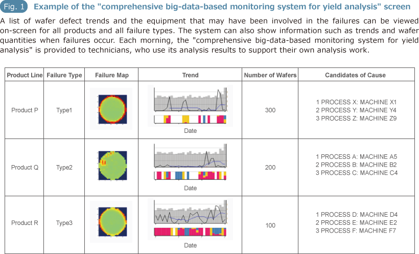
The visualization of big data produced work efficiency improvements, but analyzing which processes resulted in poor yields took even experts six or more hours per issue. We developed an automation system, called the " comprehensive big-data-based monitoring system for yield analysis " that combined big data and AI to shorten analysis time as much as possible while improving decision levels. This system could automatically categorize the distribution of failure that occurred on the wafers, which until now had been visually inspected by technicians, making it easy to analyze which processes the failures had occurred in and what equipment was involved. These results were truly the fusion of the Corporate Research & Development Center's AI core technologies and Toshiba Digital Solutions' big data and AI application technologies. This "comprehensive big-data-based monitoring system for yield analysis" dramatically reduced analysis time to under 2 hours, 1/3 as long as it had previously taken (Fig. 1).
Defect inspection
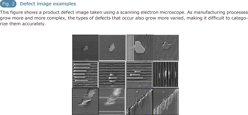
Defects on wafers are a major cause of yield loss. However, as manufacturing processes grow more and more complex, the types of defects that occur also grow more varied, making it difficult to categorize them accurately (Fig. 2).
A system for automatically classifying defect images by scanning electron microscopy exists from the past, but it can be accurately classified into 50% of the whole. The other half were classified by human eyes.We developed a new defect image classification system that used deep learning to accurately identify the delicate, complex shapes of defects. This improved the automated determination rate from 50% to 83%.
In addition to yield analysis and defect inspection, the Yokkaichi Operations also use AI support in many areas requiring high level expertise, such as product quality prediction, automatic determination of equipment maintenance timing, and the like.
With its AI, the Yokkaichi Operations have the advanced competitive capabilities necessary to consistently meet the needs of the market. Toshiba will continue to constantly innovate and make improvements in line with the changing times, using the results in customers' digital transformation.
* BiCS FLASH is a trademark of Toshiba Memory Corporation.
* The corporate names, organization names, job titles and other names and titles appearing in this article are those as of February 2018.