
Overview
TOKYO—Toshiba Corporation (Toshiba) and Toshiba Information Systems (Japan) Corporation (Toshiba Information Systems) have developed an innovative optical inspection technology that can instantly, from a single image, visualize nano-scale*1 height differences in surface defects, such as scratches, as 3D shapes on product surfaces. Toshiba Group’s current optical inspection technology, already applied across various inspection devices, detects defects at the microscale*2 defects, but the new technology extends this capability to nano-scale defects, a thousand times smaller. It is suitable for semiconductor manufacturing, where extremely minute defects must be detected instantly, and will improve inspection efficiency and yield rates.
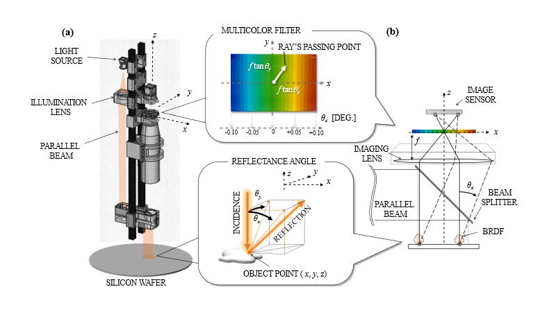
The technology is based on proprietary optical imaging systems and utilizing color filters. By replacing a standard concentric-circle color filter*3 with a multi-colored stripe filter, the system can capture the angular distribution of reflected light over a large field of view in a single shot. This algorithm utilizes a proprietary unsupervised deep neural network (hereinafter, “DNN”) that does not require pre-training, efficiently reconstructing the 3D shape of ultra-microscopic surface defects.
Application of this technology to silicon wafers used in semiconductor production has confirmed that it instantly produces 3D visualizations of nano-scale defects, surpassing the detection limits of previous methods.
Details of the breakthrough will be documented in the open-access journal Optics Continuum, published by the OPTICA organization*4.
Development background
With global expansion of demand driven by advances in digitization, generative AI, and the adoption of electric vehicles (EVs), the semiconductor industry faces increasing expectations to improve production efficiency and yield rates. Additionally, early defect detection to reduce material and energy use by minimizing defective product losses is becoming crucial for sustainability.
Toshiba has long been dedicated to developing one-shot optical inspection technologies for visualizing microscopic defects. Among optical inspection methods, area cameras are well-suited for inspecting large surface areas, while line cameras excel in inspecting products moving continuously along a production line. Toshiba has pioneered the development of OneShotBRDF™ technology, which captures reflected light distribution as bidirectional reflectance distribution function (BRDF) data. This technology was developed for area cameras in 2019*3 and adapted for line cameras in 2022*5, with sales promoted by Toshiba Information Systems*6.
Both technologies detect micro-scale height differences. However, semiconductor wafers require even higher detection precision for effective repair work, including accurate assessment of the depth, size and shape of nano-scale defects.
White light interference methods can detect such nano-scale defects, but involve scanning multiple images along the optical axis of the objective lens, and they also require complex, time-consuming image processing.
Toshiba and Toshiba Information Systems addressed these challenges by developing an area camera-based solution capable of instantly visualizing nano-scale 3D defects, particularly for applications like semiconductor wafer inspection.
Features of the technology
Toshiba and Toshiba Information Systems have developed an optical inspection technology capable of detecting extremely small defects with nano-scale height differences. This technology enables the visualization of the 3D shape of an object's surface across a field of view spanning several tens of millimeters from a single captured image. The breakthrough was achieved by utilizing multi-colored stripe filters in place of standard concentric-circle filters.
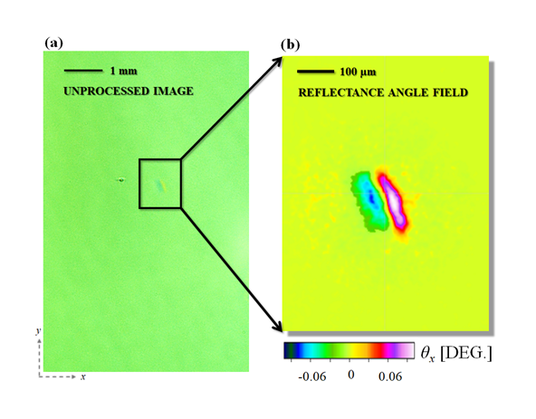
The new technology consists of an optical system that captures a field of view covering several tens of millimeters in a single shot (one-shot) and a multi-colored stripe-shaped color filter. It acquires the directional distribution of reflected light from the object being inspected as a color distribution image. The distribution of reflected light is described by the BRDF function, and adoption of a stripe-shaped color filter (Figure 1) establishes a relationship that directly corresponds to the angle of reflected light and the type of color. This makes it possible to capture the angular distribution of reflected light with higher precision (Figure 2).
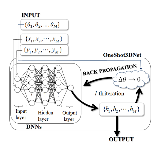
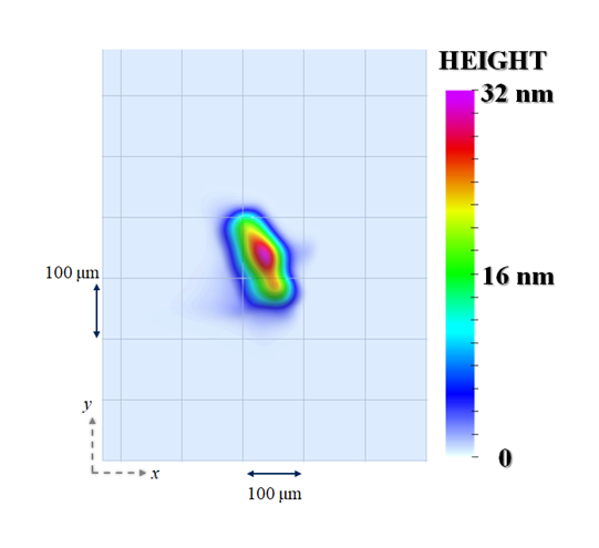
Toshiba has also developed a unique calculation algorithm that processes the angular distribution of reflected light and outputs the 3D height distribution of the object's surface. This algorithm is implemented using a DNN (Figure 3) and does not require exposure to training data. Instead, it learns the relationship between surface tilt angles and height distribution through physical formulas. This enables the reconstruction of complex 3D surface shapes, with a margin of error within a few nanometers, ensuring sufficient precision for accurate defect inspection (Figure 4).
Inspection methods that use white light interference require the capture of multiple images to measure the 3D shape of a surface. In contrast, the newly developed technology reconstructs the nano-scale 3D shape instantly from a single captured image. This simplifies the inspection process and reduces the computational load for image processing. As a result, it is expected to significantly shorten inspection times, thereby enhancing the efficiency of inspection processes and improving yield rates in semiconductor manufacturing.
Future developments
Moving forward, efforts will focus on enhancing the overall effectiveness of the technology as a complete system, with the aim of achieving its early implementation in semiconductor production processes.
- 1 nanometer is one-millionth (1/1,000,000) of a millimeter in length.
- 1 micrometer is one-thousandth (1/1,000) of a millimeter in length (1 nanometer is one-thousandth (1/1,000) of a micrometer in length).
- https://www.global.toshiba/jp/technology/corporate/rdc/rd/topics/19/1911-01.html (Available in Japanese only)
- https://doi.org/10.1364/OPTCON.541291
- https://www.global.toshiba/jp/technology/corporate/rdc/rd/topics/22/2208-01.html (Available in Japanese only)
- Toshiba Information Systems (Japan) Corporation
https://www.tjsys.co.jp/english/embedded/esb-oneshotbrdf/