
Toshiba's Advance in Gate-Insulating Film Process Technology Decreases Resistance in SiC-MOSFETs
-Next Generation Power Device Technology Reduces Power Consumption and CO2 Emissions-
Toshiba Corporation
TOKYO─Toshiba Corporation (TOKYO: 6502) today announced an advance it its gate-insulating film process technology for SiC-MOSFETs, widely seen as the core technology for next generation semiconductor power device, that cuts resistance in the channel region. Applied to actual vertical devices, the technology reduces resistance by approximately 40% against current technology, and once in practical use, it is expected to lower power loss in power inverters for cars, trains, solar cells, elevators, and devices in many other fields. Such reductions will help reduce both power consumption and CO2 emissions.
Details of this technology will be announced at the 31st IEEE International Symposium on Power Semiconductor Devices and ICs (ISPSD) in Shanghai today.
Metal-oxide-semiconductor field-effect transistors (MOSFETs) fabricated on silicon carbide (SiC), which has material properties superior to those of conventional silicon (Si), are already used in power inverters for cars, rolling stock, solar cells, elevators, and other applications that require high efficiency, and compact, light packages. However, current SiC-MOSFETs have high resistance in the channel region, the part of the circuit through which electricity flows. This has created an obstacle to reducing power loss during use, and the semiconductor industry has long recognized the need for new semiconductor process technologies to lower the resistance.
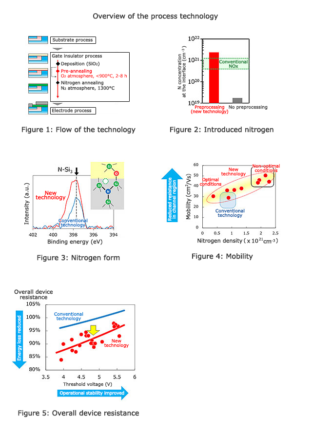
Toshiba's new process technology for the gate-insulating film in the channel region replaces widely used nitric oxide (NO, N2O) gas with nitrogen (N2) gas, which is non-toxic and easier to handle. The silicon dioxide (SiO2) film deposited on the SiC substrate is first exposed to oxygen at a low processing temperature (<900℃) prior to annealing(Note 1). Despite the low reactivity of N2 gas, the Toshiba process produces sufficient nitride in the film and cures defects around the channel region, the primary causes of increased resistance.
Compared with current processes, Toshiba's technology reduces resistance by approximately 40% in the channel region and by about 9% in the SiC-MOSFET overall. This secures reductions in power loss during device use.
Toshiba will continue its R&D on the technology toward further improving quality and promoting practical application.
- (Note 1)
- A treatment in which a material is first heated to and held at a target temperature, then cooled under conditions that result in a nearly uniform structure when it returns to room temperature.