Toshiba Develops a Gate dielectric Process Technology for Improving the Reliability of GaN-MOSFET
Toshiba Corporation
Overview
Toshiba has developed a gate dielectric process technology for improving the reliability of GaN power devices, which are expected to be the next generation of semiconducting power devices. Application of this technology will greatly reduce the variation in characteristics such as threshold voltage. The use of GaN-MOSFETs with this technology is expected to improve the reliability of GaN power devices and contribute to their further spread. The details of this technology will be presented at the International Electron Devices Meeting (IEDM) in San Francisco on 6 December 2017.
Background of This Development
Power devices that use silicon (Si) have conventionally been used in the power supplies of electrical equipment such as switching power supplies and server power supplies. Power supply efficiency is expected to be increased by using transistors made of gallium nitride (GaN), which has excellent properties as a semiconducting material.
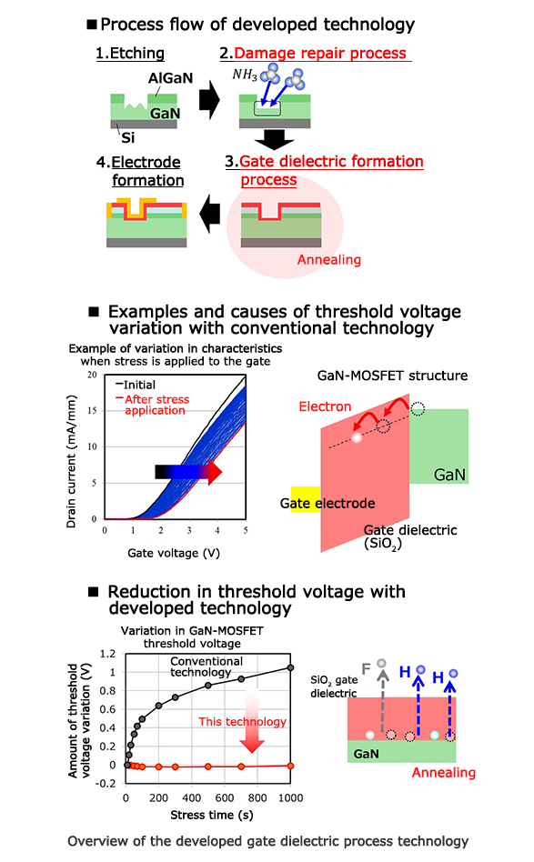
GaN-MOSFETs offer excellent speed but have suffered from the problem of threshold voltage variation with conventional technology. Consequently, GaN-MOSFETs have not come into practical use.
Features of This Technology
Toshiba has traced the cause of variations in GaN-MOSFET threshold voltage to impurity traps within the gate dielectric, and has developed a process technology that can greatly reduce impurities in the gate dielectric. Impurities such as hydrogen in the gate dielectric are substantially reduced by treatment to repair the damage that occurs during GaN semiconductor fabrication and then performing appropriate annealing of the gate dielectric. Compared with conventional technology, this greatly reduces variation in threshold voltage and delivers world-leading gate reliability.

Future Development
Toshiba is working on research and development with the aim of further increasing reliability in order to bring this technology into practical use.


