
Toshiba's New Gate Insulation Film Process Technology Cuts Resistance in SiC-MOSFETs
Toshiba Corporation
Overview
Toshiba has developed a new gate-insulating film process technology for SiC-MOSFETs that reduces resistance in their channel region by about 40%, and that is expected to reduce total device resistance by as much as 20%. SiC-MOSFETs are widely seen as next generation, advanced semiconductor power devices, and this reduction of power consumption will contribute to their adoption. Details of the technology was announced at the International Conference on Silicon Carbide and Related Materials (ICSCRM) in Washington DC, on September 18.
Development Background
Metal-oxide semiconductor field-effect transistors (MOSFETs) fabricated on silicon carbide (SiC) have superior material properties to silicon (Si), and are already used in power inverters for rolling stock and electric vehicles, which require high level efficiency and compact, light packages. However, current SiC-MOSFETs have high overall resistance, largely due to the high resistance in their channel region, a roadblock to reducing their power consumption. The semiconductor industry has long recognized the need for semiconductor process technologies that can secure lower resistance in the channel region.
Features of This Technology
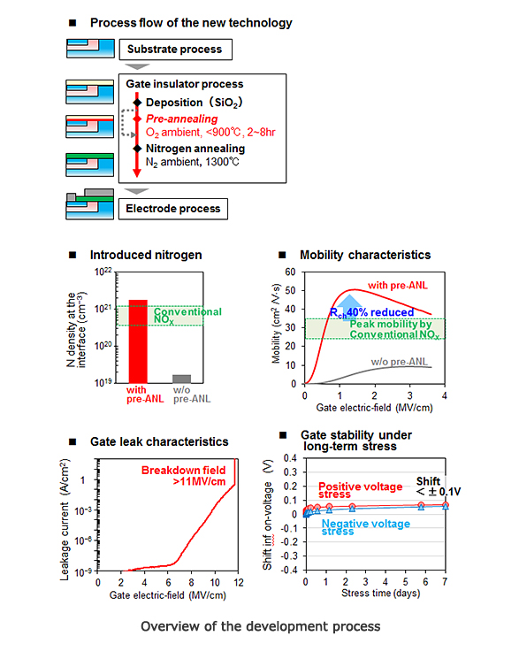
Toshiba's new technology for forming the gate-insulating film is based on nitrogen (N2) gas annealing of silicon dioxide (SiO2) as the base material for the gate-insulating film, not today's widely used nitric oxide (NO, N2O) gas annealing. Prior to the annealing process, the base material is exposed to ambient oxygen at a low process temperature (< 900℃), and this overall process achieves efficient nitridation of the film, despite the poor reactivity of the N2 gas, and cures defects around the channel region that are the primary cause of the high resistance.
Toshiba has confirmed that application of the new process technology reduces resistance in the channel region of SiC-MOSFETs by about 40% (compared with devices treated with NO gas) without any compromise to the reliability of the gate-insulating film. This can reduce the total resistance in devices by up to 20%, and secure lower power consumption in actual operation.
Future development
Toshiba will continue R&D of the technology to improve reliability and to realize practical application by 2020.