
Toshiba Develops Two-dimensional Crystallinity Characterization Technology for Directly Assessing Relationship between Performance and Crystal Structure of Nano-sized Polycrystalline Silicon Thin-film Transistors
Overview
Toshiba has developed an evaluation technology for visualizing the relationship between the performance of electron conduction channels (current paths) and crystal structures in nano-sized polycrystalline silicon(Note 1) thin-film transistors. This technology allows direct evaluation of relationship between electrical characteristics and crystal structures in polycrystalline silicon transistors in electronic devices, which are difficult to elucidate by conventional methods, and the identification of factors in the deterioration of electrical properties. Details of the technology were announced on April 6, 2017 at the International Reliability Physics Symposium (IRPS 2017) in Monterey, CA, USA.
Development Background
The spread of the Internet of Things has created demand for compact, high-performance electronic devices, such as sensors and communications devices, and accelerated development of electronic devices with three-dimensional structures, including high-performance, high-density circuits. Transistors in three-dimensionally structured devices replace conventional single-crystal silicon with stackable polycrystalline silicon thin-film. However, polycrystalline silicon has a non-uniform crystal structure, which potentially degrades electrical property (drive current). The crystal structure of the channel region is particularly important in improving the performance of polycrystalline silicon thin-film transistors, so there is a need for methods to characterize the crystal structure of polycrystalline silicon in three-dimensional nano-sized fine elements.
Features of the Technology
Toshiba developed a method for analyzing the crystal structure of polycrystalline silicon in the channel part of transistors. The channel region of polycrystalline silicon transistors is first extracted and samples are fabricated for analysis. Using the fabricated samples, the same crystallinity regions of polycrystalline silicon were successfully visualized by two-dimensional acquisition and analysis of electron diffraction patterns(Note 2), using electron microscopes with resolving powers of several nanometers or less.
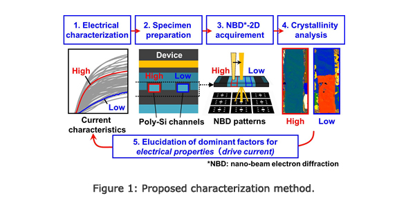
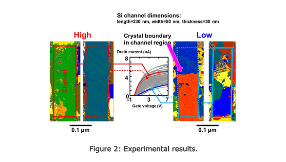
Using this characterization method, Toshiba has shown for the first time(Note 3) that the performance of polycrystalline silicon transistors is heavily dependent on the crystal grain size and on whether the current path of the transistor traverses grain boundaries (interfaces between crystals).
Future Developments
Toshiba will use this evaluation technology to improve the reliability of polycrystalline silicon transistors with three-dimensional structures. The company aims to extend the technology's pinpoint identification to various devices containing polycrystalline materials, allowing application in a broad range of fields, such as specifying the location of defective parts.
- (Note 1)
- Polycrystalline silicon: Silicon crystal composed of many small crystals. An interface called the crystal grain boundary exists between individual microscopic crystals.
- (Note 2)
- Electron diffraction pattern: An interference pattern obtained by applying an electron beam to a sample.
- (Note 3)
- According to Toshiba's investigation.