

December 5, 2016
Bureau of Science, Technology and Innovation, Cabinet Office
Tel : 03-6257-1339
Toshiba Corporation
Tel : 03-3457-2100 (PR & IR Division)
National Institute of Advanced Industrial Science and Technology (AIST)
Tel : 029-862-6216 (Media Relations Office)
Japan Science and Technology Agency (JST)
Tel : 03-5214-8404 (Public Relations Department)
Development of new voltage-controlled writing method for nonvolatile solid-state magnetic memory
Road to achieving ultra-low-power high-speed "voltage torque MRAM"
Key Points
- A new voltage-controlled writing method has been devised for nonvolatile magnetoresistive random access memory (MRAM).
- A new circuit has been developed that reduces error rate of voltage-controlled writing.
- This technology provides a path for applying voltage torque MRAM to ultra-large last-level caches.
As part of the Impulsing PAradigm Change through disruptive Technologies Program (ImPACT) (Program Manager: Masashi Sahashi) led by the Council for Science, Technology and Innovation of the Cabinet Office, an R&D team consisting of Shinobu Fujita, the Chief Research Officer of Toshiba Corporation's Corporate Research & Development Center (Center Director: Osamu Hori) and Takayuki Nozaki, Leader of the Voltage-driven Spintronics Team, Spintronics Research Center (Director: Shinji Yuasa), National Institute of Advanced Industrial Science and Technology (AIST; Director: Ryoji Chubachi), have developed a new write method that reduces the write error rate of "voltage torque MRAM," which is a type of voltage-controlled nonvolatile magnetic memory.
The Voltage-driven spintronics team in AIST previously developed a magnetic tunnel junction (MTJ) element, in which magnetization reversal can be controlled by fast voltage pluses, and has been developing a new type of voltage-controlled magnetic memory, "voltage torque MRAM." Voltage torque MRAM is expected to offer dramatically lower power consumption than conventional current-controlled magnetic memory (STT-MRAM), but reducing the write error rate has been a major challenge in terms of practical application of the technology.
In this work, the AIST team and an R&D team in Toshiba developed a method that suppresses the occurrence of write failures due to thermal fluctuations and reduces the write error rate by applying pulse voltage with the reversed polarity of the write voltage before and after the pulse voltage applied during writes. A new write circuit has also been developed to implement this method. This result is expected to lead to larger capacity last-level caches and increased processor performance.
The technical details of this result will be presented at the International Electron Devices Meeting (IEDM) on 7 December 2016 in San Francisco, California. The results will be published in the "IEDM 2016 Technical Digest" scheduled for release at 1:30 PM on 3 December 2016 (Pacific Standard Time).
These results were obtained from the following programs and research and development topics.
Impulsing PAradigm Change through disruptive Technologies Program (ImPACT), Cabinet Office https://www.jst.go.jp/impact/
- Program Manager :
- Masashi Sahashi
- R&D Program :
- Achieving Ultimate Green IT Devices with Long Usage Time without Charging
- R&D Topics :
- Circuit design for voltage-controlled MRAM
- Principal Investigator :
- Shinobu Fujita (Chief Research Officer, Corporate Research & Development Center, Toshiba Corporation)
- R&D Period :
- FY 2016 to 2018
- R&D Topics :
- Development of new material elements for voltage-controlled MRAM
- Principal Investigator :
- Takayuki Nozaki (Leader, Spintronics Research Center, AIST)
- R&D Period :
- FY2016 to 2018
- R&D Topics :
- Development of process technology and memory arrays for voltage-controlled MRAM
- Project Leader
/Principal Investigator : - Shinji Yuasa (Director, Spintronics Research Center, AIST)
- R&D Period :
- FY2016 to 2018
For these R&D topics, the work is being done on verifying memory operation, developing circuits for voltage control, and developing materials and process technologies in order to realize voltage-controlled MRAM.
■Comments from Program Manager Masashi Sahashi■

These results will be presented at the International Electron Devices Meeting held in San Francisco, California, on 3-7 December 2016. Toshiba would like to build on the momentum of these results and work through industry-government-academia cooperation toward resolving problems in respect of practical application and further accelerating activities aimed at market expansion.
Research Background and Process
Reducing the power consumption of IT devices is of prime importance in terms of conserving the global environment while providing the richness of social activity. In the field of electronics, a key technology that is attracting a great deal of attention for achieving these goals is nonvolatile memory that does not require power to store data. In the field of spintronics, development has been progressing on "MRAM" nonvolatile magnetic memory that utilizes the nonvolatile nature of magnets and is recognized as the only nonvolatile memory offering high capacity, high speed, and highly repeatable operation. However, presently available magnetic memories are "current-controlled," which means that data are written (i.e. magnetization is reversed) by supplying current to the MTJ element. This creates the problem that power consumption for writing is larger in the magnetic memory than in semiconductor memory. To fundamentally resolve this problem, the Voltage-driven Spintoronics team has been working on developing "voltage torque MRAM", which is voltage-controlled and uses an extremely small amount of power during writing. This type of MRAM, which requires zero stand-by power and very little active power, is being developed through the ImPACT project "Achieving Ultimate Green IT Devices with Long Usage Time without Charging (Program Manager: Masashi Sahashi)".
The Voltage-driven Spintoronics team previously worked on developing technology for control of magnetic anisotropy by applying voltage to ultra-thin metallic magnetic films, as well as new magnetization reversal control methods that use this technology (refer to the JST press release of 10 December 2015, "Proof of Stable Operation of Voltage Write Method Nonvolatile Memory and Evaluation of the Write Error Rate"). One thing that is particularly important for making voltage torque MRAM practical is minimizing the failure rate when writing data (i.e., minimizing the write error rate). The above-mentioned press release details material design guidelines for achieving an error rate of 10-10 to 10-15 as a rough guide for practical application, and ImPACT is currently making progress in developing materials that following these guidelines.
In the present work, the Voltage-driven Spintronics team in AIST and the R&D team in Toshiba developed methods for reducing the write error rate and performed circuit design that achieves a low write error rate by improving material characteristics through the mechanism of applying a pulse voltage having a devised waveform during writing.
Research Details
Figure 1 shows schematic diagrams of (a) the conventional method and (b) the new method for voltage-controlled writing. In Fig. 1(a), the magnetization stabilizes in the downward facing (or upward facing) direction, where the magnetic anisotropy energy is the lowest when a voltage is not applied. In this way, 1 bit of data is stored in a nonvolatile manner. Then, when a positive voltage pulse is applied, the magnetization starts rotational motion due to the magnetic anisotropy instantly becoming zero. If the pulse voltage is shut down exactly when the magnetization is facing the opposite direction from the initial state, the magnetization can be reversed to the upward facing (or downward facing) stable point at the opposite side, and thus the data is written. This gives the basic operation of magnetization reversal (i.e. writing data) by voltage. Note that the magnetization direction fluctuates both in the initial state before the magnetization reversal and in the final state after the reversal because of thermal energy. As the thermal fluctuations become larger, write error rate can increase. In other words, the write error rate can be reduced by suppressing thermal fluctuations of the magnetization in the initial and final states.
The basic method for minimizing the thermal fluctuations is to use a metal magnetic material with a large magnetic anisotropy to increase the stability to the magnetization against thermal energy, but there are limits to merely improving the metal magnetic material.
The method newly developed in this work reduces the write error rate by using voltage to increase the perpendicular magnetic anisotropy. Figure 1(c) shows a schematic of changing the magnetic anisotropy by using voltage. Because the magnetic anisotropy changes linearly as a function of applied voltage, it becomes smaller for positive voltages and larger for negative voltages. In conventional voltage writing, magnetization reversal is performed by using only the reduction in magnetic anisotropy by application of a positive voltage pulse. In the new method, on the other hand, the write error rate is greatly reduced by suppressing thermal fluctuations of magnetization in the initial and final states by applying a negative voltage in these states, thereby increasing the magnetic anisotropy as shown in Fig. 1(b).
Note that to implement the above method, it is necessary to accurately apply a pulse voltage that has a pulse width of around 1 nanosecond and steep reverse polarity of around several hundred picoseconds to each of the elements within the memory array. In circuits for writing conventional magnetic memory, it has been difficult to generate high-speed voltage pulse with an accurately controlled waveform, because the waveform of the voltage pulses can be degraded because of the influence of resistance and capacitance components of memory elements and wiring, which make the quick switching of the voltage polarity difficult. The team therefore developed a special write circuit for voltage torque MRAM that can generate fast pulse voltages with reverse polarity. Figure 2(a) shows an overview of the fast voltage pulse generation. The three stages of the pulse voltages that will be switched between at high speed are set up in advance on three wires (called dummy bit lines A, B, and C). Each of these wires has a loop structure with respect to the write instruction (trigger signal), where the next signal is triggered by previous signal. In other words, this is a mechanism that applies each of the wires to the element sequentially in the order A → B → C. This enables the write pulse voltage to be accurately controlled at high speed without delays or loss of the waveform shape. Figure 2(a) shows an example for A= 0 V, B = 1.5 V, and C = 0 V, which can generate a 1.5 V pulse voltage with extremely steep rising (and falling) edges and short pulse width (A and C can also be set to values other than 0 V). At this point, if a voltage of 1 V, for example, is applied to the reverse side bit lines, then the actual voltage signal applied to the element will be -1 V → 0.5 V → -1 V, and it would be possible to accurately apply a high-speed pulse with reverse polarity (Fig. 2(b)).
Furthermore, memory circuit operation time can be reduced by simultaneously performed reading while applying the reverse polarity pulse voltage. This makes it possible to read the recorded data of the initial state and instantly skip the write process if there is no need to write the data, and also to quickly perform the error correction process called "verify", in which the recorded data is checked again after writing and is written again in the event of a write error. Combination of these error rate reduction methods can achieve the target error rate of 10-10 to 10-15 for practical applications.
In addition to reducing the write error rate, the team also developed a new read circuit that utilizes the phenomenon where the resistance of the MTJ element changes for read voltages.
Great improvement in write and read error rates was demonstrated by leading-edge CMOS circuit simulations based on measurement data for a fabricated memory element of diameter 30 nm. It was shown that if the efficiency of the voltage-controlled magnetic anisotropy can be enhanced by three times than the present value, it will be possible to apply this technology in ultra-large last-level caches with memory capacities of 1 to 2 Gbit.
Future Development
The Voltage-Spintronics team in AIST and the R&D team in Toshiba is aiming to demonstrate voltage-controlled magnetic anisotropy that satisfies the requirements for large-capacity last-level cache or even larger capacity main memory in actual MTJ elements of several tens of nanometers, based on the new directions opened by this research. And further development for higher performance circuit systems will also be continued.
Reference Diagrams
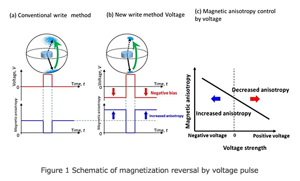
(a) Write method using conventional pulse voltage. The black arrows show the orientation of the magnetization of the ferromagnetic metal layer of the MTJ element. The magnetic anisotropy is reduced by applying the pulse voltage and the magnetization reverses from downward facing to upward facing. The magnetization orientations of the initial and final states fluctuate in the cyan regions due to thermal energy, and it can increase write failures. (b) The new write method. The magnetic anisotropy of the ferromagnetic metal layer is increased by applying a reverse polarity voltage before and after writing, which reduces the write error rate by suppressing the thermal fluctuations. (c) Overview of the changes in magnetic anisotropy by voltage
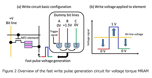
(a) Circuit for generating fast pulse voltages that allow for polarity reversal. The fast pulse voltage is generated by putting the supply voltages from the dummy bit lines, which are set to the designated voltages in advance, into a loop structure and switching through them in the sequence (1) → (2) → (3). (b) A fast pulse voltage with polarity reversal can be applied to the element depending on the magnitude relationship between the voltages applied from the bit lines.
Glossary
(Note 1) Write error rate
In general, when memory is written, there is some probability of write errors occurring. The probability with which write errors occur is called the "write error rate." For example, an error rate of 10-3 means that an error occurs once for every 1000 write operations. Low error rates of around 10-12 to 10-15 are demanded of fast memory applications for DRAM and SRAM hierarchies. If the memory write error rate is large, the write error rate can be lowered by error correction operations that check whether an error has occurred immediately after the write operation and performs the write again if an error occurred.
(Note 2) Voltage torque MRAM
Magnetic memory that performs recording of data in a nonvolatile way by using the two stable resistance value states of MTJ elements is called MRAM (magnetoresistive random access memory). In existing magnetic memory (called STT-MRAM), writing of data (magnetization reversal) is performed using current. In contrast, to greatly reduce the power consumption during writes, the development of MRAM magnetic memory that uses a new write method based on magnetization reversal induced by voltage is being actively pursued. This is called voltage torque MRAM (or voltage-controlled MRAM).
(Note 3) Magnetic tunnel junction(MTJ) element
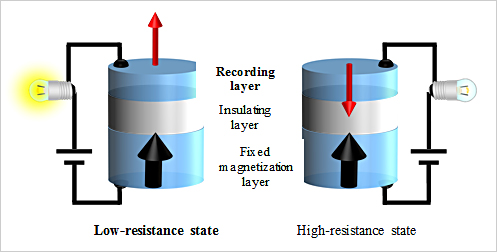
When a voltage is applied to both sides of an MTJ element with a configuration of magnet/insulating layer/magnet and a film thickness of several nanometers, a small tunnel current flows through the insulating layer due to quantum mechanical effects. The ease with which the tunnel current flows varies greatly, depending on the relative angle between the magnetizations of the magnets on both sides, known as the tunneling magnetoresistance effect. In general, the resistance is low when the magnetizations are parallel and high when the magnetizations are antiparallel. A single bit of data can be recorded in a nonvolatile way by using these two value states. High-performance MTJ elements using magnesium oxide (MgO) for the insulating layer material were developed by AIST in 2004, and form the core technology of currently available magnetic memories and magnetic sensor elements. Furthermore, "perpendicularly magnetizatized MTJ elements," which use a perpendicularly magnetized material for the ferromagnetic metal layers in combination with the MgO insulating layer, were developed by Toshiba in 2007, and are now the main-stream technology for STT-MRAM.
(Note 4) Magnetization reversal
Reversal of the orientation of the magnetization of a magnet (from the S pole to the N pole). In magnetic memory, data are written by magnetization reversal of the ferromagnetic metal layer that forms the recording layer of MTJ elements.
(Note 5) STT-MRAM
MRAM that uses the current write method is called "STT-MRAM" (spin-transfer-torque MRAM), and progress is currently being made in product development around the world. The digital information (0's and 1's) in the storage-layer is overwritten by changing the direction of the current flowing in the MTJ memory element.
(Note 6) Spintronics and spintronics devices
Electronics technology that uses magnetic bodies is called spintronics. Spintronics uses "spin," which is a natural property of the electrons that creates magnets, together with electrical charge to create electronic devices that have new functions that could not be realized with previous technologies. Electronic devices that use spintronics are called spintronic devices, with major examples including the magnetic read heads in ultra-high density hard disk drives and MRAM.
(Note 7) Magnetic anisotropy
This is a phenomenon where the internal energy of a magnet differs depending on the orientation of the magnetization inside the magnet, and determines the easy axis of magnetization. This is normally a fixed property arising from factors such as the crystalline structure and shape of magnet, however in recent years it was discovered that magnetic anisotropy can be controlled by applying a voltage to an ultra-thin ferromagnetic metal layer, and this has attracted attention as a new method for controlling magnetization reversal.
(Note 8) Last Level Cache
Advanced processors use multi-level cache memory such as level-1 cache, level-2 cache, level-3 cache etc. The number of level depends on applications. Last level cache is the cache memory having the largest number of the level.
Name of Paper
IEDM 2016 (International Electron Devices Meeting), 7 December 2016 (Wednesday)
27.5 "Novel Voltage Controlled MRAM (VCM) with Fast Read/Write Circuits for Ultra Large Last Level Cache"
Published also in the IEDM 2016 Technical Digest on 3 December 2016.
Inquiries
Research
Corporate Research & Development Center, Toshiba Corporation
1 Komukaitoshiba-cho, Saiwa-ku, Kawasaki, Kanagawa 212-8583, Japan
Tel: 044-549-2056
ImPACT program
ImPACT Program Promotion Office, Cabinet Office
1-6-1 Nagatacho, Chiyoda-ku, Tokyo 100-8914, Japan
Tel: 03-6257-1339
ImPACT details and project management
Office for the Impulsing Paradigm Change through Disruptive Technologies Program, JST
K's Gobancho, 7 Gobancho, Chiyoda-ku, Tokyo 102-0076, Japan
Tel: 03-6380-9012 Fax: 03-6380-8263
E-mail: impact@jst.go.jp
Press relations
Public Relations Department, JST
5-3 Yonbancho, Chiyoda-ku, Tokyo 102-0081, Japan
Tel: 03-5214-8404 Fax: 03-5214-8432
E-mail: jstkoho@jst.go.jp
PR & IR Division, Toshiba Corporation
1-1, Shibaura 1-Chome, Minato-ku, Tokyo 105-8001, Japan
Tel: 03-3457-2100
Media Relations Office, Planning Headquarters, AIST
AIST Tsukuba Central 1, 1-1-1 Umezono, Tsukuba, Ibaraki 305-8560, Japan
Tel: 029-862-6216 Fax: 029-862-6212
E-mail: press-ml@aist.go.jp