

December 5, 2016
Bureau of Science, Technology and Innovation, Cabinet Office
Tel : 03-6257-1339
Toshiba Corporation
Tel : 03-3457-2100 (PR & IR Division)
Japan Science and Technology Agency (JST)
Tel : 03-5214-8404 (PR Department)
Proposal & demonstration of a new writing method for nonvolatile magnetic memory using voltage-control magnetization reversal
Demonstration of major improvement in write error rate showing the possibility of the ultimate low-power memory with large-capacity
Key Points
- Development of a new architecture technology, voltage-control spintronics memory (VoCSM), for voltage-write nonvolatile magnetic memory that uses two new physical principles of spintronics, voltage-control magnetic anisotropy (VCMA) effect and the spin Hall effect, to write data.
- Demonstration of batch writing of multiple bits by a unique write sequence, voltage-control flash (VoCF) writing, that makes innovative use of selective magnetization reversal by the VCMA effect and shows the possibility of reducing write power consumption by one order of magnitude.
As part of the R&D program managed by Prof. Masashi Sahashi in the Impulsing PAradigm Change through disruptive Technologies Program (ImPACT) led by the Council for Science, Technology and Innovation of the Cabinet Office, an R&D team consisting of Senior Fellow Hiroaki Yoda and co-workers of the Corporate Research & Development Center of Toshiba Corporation have developed a new architecture technology for voltage-write nonvolatile magnetic memory.
Toshiba has successfully developed a new architecture technology that is able to secure a low write error-rate, which had previously been a problem for realizing voltage-write nonvolatile magnetic memory using voltage-control magnetization reversal. The team has developed a unique architecture technology (VoCSM) for voltage-write nonvolatile magnetic memory that uses two new physical principles of spintronics, the VCMA effect and the spin Hall effect, to write data. Batch writing of multiple bits has also been demonstrated by using a unique write sequence (VoCF writing). This demonstrates the possibility of reducing the power consumption during writing by an order of magnitude while securing a low write error-rate.
The results achieved show the possibility of implementing voltage-write nonvolatile magnetic memory, which is the ultimate in low-power, large-capacity memory and ultra-low-power IT devices.
Moving forward, Prof. Masashi Sahashi's program will work on improving the VCMA effect, the biggest hurdle with respect to practical application of the technology, in cooperation with the National Institute of Advanced Industrial Science and Technology (AIST), the National Institute for Materials Science (NIMS), Tohoku University, Osaka University, and Toshiba.
The technical details of these results will be presented at the International Electron Devices Meeting (IEDM 2016) being held on 7 December 2016 in San Francisco, California. Furthermore, the research results will be published in the "IEDM 2016 Technical Digest" scheduled for release at 1:30 PM on 3 December 2016 (Pacific Standard Time).
These results were obtained from the following programs and research projects.
ImPACT, Cabinet Office https://www.jst.go.jp/impact/en/index.html
- Program Manager :
- Masashi Sahashi
- R&D Program :
- "Achieving Ultimate Green IT Devices with Long Usage Time without Charging"
- R&D Topics :
- "Development of process technology and memory arrays for voltage-controlled MRAM"
- Principal Investigator :
- Hiroaki Yoda (Lead Engineering, Corporate Research & Development Center, Toshiba Corporation)
- R&D Period :
- 2014 to 2018
Under the above R&D topics, the work is being done on developing memory architectures, memory devices, memory elements, and the microfabrication technologies for all of these as important component technologies for implementing voltage-controlled MRAM.
■Comments from the ImPACT Program Manager Masashi Sahashi■
Research Background and Process
With continuing advances in new devices that transmit network information, such as the IoT(Note 1) and CPS(Note 2), the realization of so-called green information technology (IT) through the construction of new memory hierarchies in computer memory and the reduction of power consumption by IT devices are urgent social problems of the utmost importance that need to be tackled. One approach is the development of nonvolatile electronics devices. In the field of spintronics(Note 3), active work is being done on the development of MRAM nonvolatile magnetic memory, which achieves zero standby power(Note 5) by using a magnetic tunnel junction (MTJ) memory cell(Note 4) based on the nonvolatility of the magnetization. At present, product research on current-writing MRAM (STT-MRAM)(Note 6) is progressing at the global scale, and it is expected to become a low-power nonvolatile magnetic memory. However, MRAM that uses this method requires a write current, and this imposes limits on reducing the power consumption during operation due to Joule heat.
Features of voltage-writing MRAM that uses magnetization reversal control by voltage pulses of several nanoseconds include 1) low-power operation that, in principle, requires no current; 2) fast several-nanosecond operation; 3) high durability; and 4) the ability to operate at room temperature. The voltage-writing MRAM magnetic memory is still at the stage of basic research. However, it is expected to have a large social impact when realized, because it offers significantly lower power consumption than current-writing STT-MRAM. Also, voltage-writing MRAM allows implementation of the ultimate in ultra-low power consumption nonvolatile memory and reduced transistor sizes, because it is voltage-operated, like the transistors in CMOS(Note 7), thus holding the potential for high integration densities.
To date, the ImPACT Sahashi Program has been working on a physical understanding of interfacial voltage effects and developing evaluation technologies and materials for voltage-writing MRAM. The program has focused on the development of technology for controlling the magnetization easy axis (magnetic anisotropy) by applying voltage to metal magnet thin films of several atoms thickness, with participation by the NIMS, Tohoku University Advanced Institute for Materials Research (AIMR), the Osaka University Graduate School of Engineering Science, the Japan Synchrotron Radiation Research Institute and Toshiba Corporation in the voltage-writing MRAM development task force project (Project Leader: Shinji Yuasa, Director of the Spintronics Research Center, AIST) headquartered at AIST (JST press release of 10 December 2015, Tohoku University AIMR press release of 26 July 2016, etc.).
To make voltage-writing MRAM practical, the write error-rate needs to be around 10-10 to 10-15 or lower. However, although write error-rates of the voltage pulse write method have been evaluated previously and the method has been shown to operate stably as memory (JST press release of 10 December 2015, etc.), no proposals have been put forward from the perspective of a memory architectures that reduces the write error-rate.
In this work, the Toshiba team led by Hiroaki Yoda, Senior Fellow at Toshiba Corporation's Corporate Research & Development Center and principal investigator of the ImPACT Sahashi Program, developed a new architecture technology, voltage-written nonvolatile magnetic memory (VoCSM). VoCSM uses two new spintronics physical principles (VCMA(Note 8) and the spin Hall effect(Note 9) ) to write data. A substantial improvement in the write error-rate was demonstrated by this development.
Note that this R&D was performed as part of the "Achieving Ultimate Green IT Devices with Long Usage Time without Charging" R&D program (Program Manager: Masashi Sahashi) of ImPACT under the Cabinet Office.
Research Details
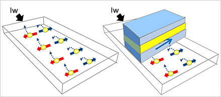
The R&D team of Toshiba has proposed a new architecture technology (VoCSM) for voltage-write nonvolatile magnetic memory, fabricated a prototype unit memory cell that uses it, and shown the possibility of greatly improving the write error-rate. Furthermore, the Toshiba team has also demonstrated a unique low-power batch write sequence called VoCF writing and shown the possibility of reducing write power by an order of magnitude.
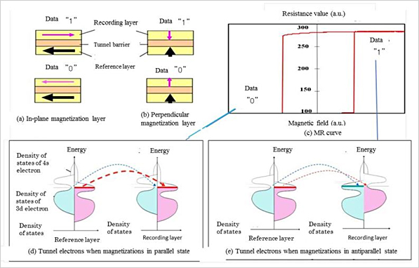
The VoCSM memory element uses the mature technology of MTJ memory elements and uses the TMR effect(Note 10) for reading data, in the same way as conventional MRAM. The data writing technology at the heart of this R&D uses this new VoCSM architecture for voltage-writing nonvolatile magnetic memory based on two new physical principles of spintronics─the VCMA effect and spin Hall effect.
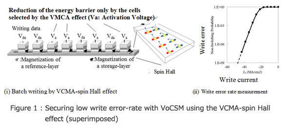
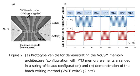
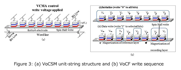
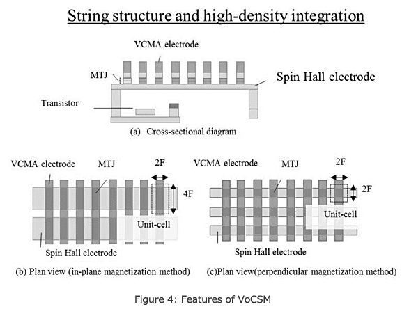
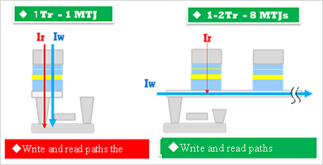
By using a method that combines the spin Hall effect and the VCMA effect, the Toshiba team has demonstrated for the first time the possibility of greatly lowering the write error-rate (Figure 1). Furthermore, Toshiba has demonstrated that multiple bits can be batch written by using the prototype vehicle (composed of a string-of-beads structure with MTJ memory elements arranged in a line) implemented using the unique VoCF writing sequence developed in this work (Fig. 2). This has shown the possibility of reducing power consumption during writing (during operation) by an order of magnitude. Note that although the new architecture presented in this work has a three-terminal structure, it avoids the drawback that a three terminal structure tends to increase the footprint by employing the string-of-beads structure, in which multiple MTJ memory elements are arranged on a single string. The VoCSM architecture and VoCF writing sequence are anticipated as technologies with potential for future capacity increases for the reasons given below.
In current-writing STT-MRAM, since a two-terminal structure is used that employs the same current paths in reading and writing, current flows through the tunnel barrier in both cases, and there is a possibility of read disturbances(Note 11) that accidentally write data during reading. As a result, it is necessary to employ a design that takes care to avoid the read disturbances and secures the reliability of the tunnel barrier during writing. The VoCSM architecture is able to eliminate the read disturbances almost entirely by selecting the polarity of the read voltage that is applied. Furthermore, because there is no write current to flow through the tunnel barrier, this eliminates the concern for the reliability of the tunnel barrier. (In principle, the durability offers an infinite number of rewrites.) Also, transistors can be made smaller because they are voltage-driven, like CMOS transistors.
If the VCMA effect can be increased without degrading other features, it will be possible to secure a broad design window and to offer superior scalability. This is the challenge that ImPACT aims to tackle.
The details of these results will be reported as a technical presentation in the Technical Session on 7 December (Wednesday) at IEDM 2016, which will be held in San Francisco, California, starting 3 December 2016 (Saturday).
Future Development
In order for the MRAM memory architecture and the batch writing method newly developed in this work to lead to practical application, it is necessary to improve the efficiency of the two physical principles of spintronics used in MTJ elements with sizes on the order of 10 nm. In particular, it is necessary to develop MTJ memory elements and materials technology that significantly increase the VCMA effect. In the future, the Masashi Sahashi program team will work to resolve this problem by strengthening cooperation between the National Institute of Advanced Industrial Science and Technology, Tohoku University AIMR, NIMS and Toshiba, under the leadership of Dr. Shinji Yuasa (Spintronic Center Director, National Institute of Advanced Industrial Science and Technology) of the ImPACT Sahashi program.
Reference Diagrams
Features of VoCSM and reasons
| Feature | Reason |
|---|---|
| Low energy consumption | Unique VoCF write sequence |
| High-density integration | Arrange multiple MTJ memory elements on a single string |
| Robust against read disturbance | The write current path differs from the read current path(essentially a three-terminal structure) |
| No limit on tunnel life | Write current does not flow through tunnel barrier. |
Glossary
(Note 1) IoT
Abbreviation for the Internet of Things. Refers to the mechanism of connecting various "things" other than IT-related equipment such as computers, servers, and printers that are conventionally connected to the Internet, for mutual control by information exchanges; also refers to the society realized by this approach.
(Note 2) CPS
Abbreviation of cyber-physical system. Refers to vitalizing industry and solving social problems by using the information generated by using sensor networks and the like to collect various data from the real world (physical space) and analyzing it by using large-scale data processing technology and other means in cyber space.
(Note 3) Spintronics
A field that attempts to create electronic devices that have new functions by using both the electrical charge (electrical property) and spin (magnetic property) of electrons.
(Note 4) MTJ memory element
MTJ is an abbreviation of magnetic tunnel junction. It is an element that consists of a storage-layer, insulating-layer, and reference-layer. The phenomenon whereby the electrical resistance of an MTJ element changes depending on the relative alignment of the magnetization directions of the two ferromagnetic layers is called the tunnel magnetoresistance effect. When the magnetizations of the storage layer and the reference layer are parallel, the resistance is low, and when they are antiparallel, the resistance is high.
(Note 5) MRAM
Nonvolatile memory that uses MTJ memory elements is called "MRAM". In MRAM, 1 bit of data is recorded by associating the high resistance state and low resistance state of the MTJ memory element with 0 and 1, respectively. Methods of writing to MRAM memory include methods using magnetic fields, method using current, and methods using voltage.
(Note 6) STT-MRAM
MRAM that uses the current write method is called "STT-MRAM" (spin-transfer-torque MRAM), and progress is currently being made in product development around the world. The digital information (0's and 1's) in the storage-layer is overwritten by changing the direction of the current flowing in the MTJ memory element.
(Note 7) CMOS
Abbreviation of complementary metal─oxide─semiconductor. Refers to a circuit system (logic system) that uses p-type and n-type MOSFETs complementarily as logic gates and so forth in digital circuits (logic circuits), and to the electrical circuits and ICs that use this system.
(Note 8) VCMA
Abbreviation of voltage-control magnetic anisotropy. Refers to an effect whereby the magnetic anisotropy changes when an electric field is applied to the surface of a magnetic body.
(Note 9) Spin Hall effect
Refers to an effect where spin-polarized electrons group together on the surface when a current is passed through a heavy metal such as Tantalum.
(Note 10) Tunnel magnetoresistance effect
Refers to an effect whereby the tunnel resistance varies depending on the magnetization configurations whether parallel or antiparallel.
(Note 11) Read disturbance
An accidental write that occurs from the read current. In the case of STT-MRAM, even though the read current (around 10μA) is small, it applies a spin torque and unintentional data-writes are possible.
In the case of VoCSM, elements can be made robust against the read disturbances by appropriately selecting the polarity of the applied read voltage (also since the read current that flows is quite small, the order of a sub micro-ampere, the spin torque is also quite small).
Excerpt from MRAM session program
27.6 Voltage-Control Spintronics Memory (VoCSM) Having Potentials of Ultra-Low Energy-Consumption and High-Density
Inquiries
Research
Corporate Research & Development Center, Toshiba Corporation
1 Komukaitoshiba-cho, Saiwa-ku, Kawasaki, Kanagawa 212-8583, Japan
Tel: 044-549-2056
ImPACT program
ImPACT Program Promotion Office, Cabinet Office
1-6-1 Nagatacho, Chiyoda-ku, Tokyo 100-8914, Japan
Tel: 03-6257-1339
ImPACT details and project management
Office for the Impulsing Paradigm Change through Disruptive Technologies Program, JST
K's Gobancho, 7 Gobancho, Chiyoda-ku, Tokyo 102-0076, Japan
Tel: 03-6380-9012 Fax: 03-6380-8263
E-mail: impact@jst.go.jp
Press relations
PR & IR Division, Toshiba Corporation
1-1, Shibaura 1-Chome, Minato-ku, Tokyo 105-8001, Japan
Tel: 03-3457-2100
Public Relations Department, JST
5-3 Yonbancho, Chiyoda-ku, Tokyo 102-8666, Japan
Tel: 03-5214-8404 Fax: 03-5214-8432
E-mail: jstkoho@jst.go.jp