
Development of Cache Memory with the Highest Power Performance in the World by Using STT-MRAM Magnetic Memory
Overview
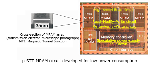
Toshiba has developed a 4-Mb-class memory circuit using STT-MRAM, a new type of magnetic memory that integrates 65-nm silicon transistors, for high-performance processors and use in system-on-a-chip (SoC) in cooperation with the research group of Professor Hiroshi Nakamura from the Faculty of Engineering at Tokyo University.
This memory circuit offers 3.3-ns memory access, which is fast enough for use as cache memory, and consumes less than 1/10th of the energy that conventional integrated memory (SRAM: static random-access memory) does. This offers the highest power performance in the world for integrated memory. The details of this technology were presented at the 2016 IEEE International Solid-State Circuits Conference (ISSCC), which will be held in San Francisco in the United States on February 2nd (local time).
Background of Development
In recent years, the semiconductor chip market has been growing as chips are used in a variety of applications, including the Internet of Things, wearables, smartphones, and desktop PCs, as well as in data center servers. At the same time, the demand for higher performance and lower power consumption has been increasing. In terms of the power consumption in these semiconductor chips, reducing the power consumption of the memory block has become a focus of development as the size of SRAM inside the chips has increased. In particular, the power consumption attributable to current leaking inside the memory (leakage current) is large, and our company has been continuing to develop magnetic tunneling junction (MTJ) non-volatile magnetic memory that offers high speed and low power consumption, with the expectation that there will be a change from the currently used volatile memory to non-volatile memory.
However, since power consumption due to memory writes and memory control circuits (peripheral circuits) is high, the overall power consumption is not low enough for use in cache memory, even for a memory array circuit that is implemented with lower power consumption (normally off(Note 1)).
Features of This Technology
In order to solve the current-related problems, our company has developed circuits capable of high-speed power shutdown-and–recovery, at sub 100-ns speeds, to allow the memory-control circuit unit to more fully achieve a normally off state, and we have made improvements that allow the power supply to be cut off at high speed in units not required to operate, according to the memory operation state. Furthermore, in order to shut down the power supply efficiently, Tokyo University and we developed an algorithm that monitors the patterns of memory access and predicts the access pattern that is highly probably to be next. This algorithm is built into the memory-control circuit. By using these technologies, we have been able to reduce the power consumption to less than 1/10th that of SRAM.
Future Developments
The technological development of the magnetic memory described here has been conducted as part of the New Energy and Industrial Technology Development Organization (NEDO) “Normally-off” computing development project, in cooperation with the research group of Professor Hiroshi Nakamura from the Faculty of Engineering at Tokyo University. Our company is continuing to further improve the new magnetic memory elements and circuits that we have already developed and to develop memory technology that is suitable for even smaller silicon transistors.
- (Note 1)
- Refers to actively shutting down the power supply to components except those that truly need to operate as a means to save power even while a system is operating.