
Development of a Wireless Receiver Architecture for Bluetooth Low Energy with the World's Lowest Power Consumption
Summary
Toshiba has developed a new radio receiver architecture that meets Bluetooth® Low Energy (BLE)(Note 1) standards. This new architecture achieves the world’s lowest power consumption by reducing the number of components in the electrical circuits of the radio receiver. Applying this technology to wearable devices will enable longer use with wireless devices. This new technology will be presented in San Francisco on February 3 (local time) at the 2016 IEEE International Solid-State Circuits Conference (ISSCC).
Development Background
Wearable devices that present useful information to the user have begun to attract attention with today' growing awareness of healthy lifestyles and the spread of the Internet of Things (IoT). These devices can easily measure information on lifestyle and health status, and they can process various types of measurement data including biological information in an integrated fashion. The data collected from wearable devices are now commonly transmitted to an external device such as a smartphone by BLE. This has generated great demand for wearable devices that have small size, light weight, and long battery life. The technology necessary to meet these requirements is a low-power wireless communication unit.
Features of This Technology
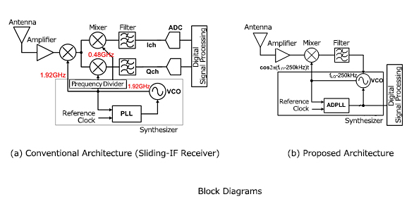
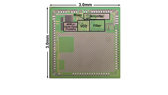
This new receiver architecture features data demodulation using an analog signal processor with a single in-phase component, rather than a conventional two-signal analog signal processor that has both in-phase and orthogonal components. This was achieved by setting the frequency of the frequency synthesizer(Note 2) of the receiver circuit.
Another feature of this architecture is that it eliminates the need for an A/D converter(Note 3) in demodulation processing. This was achieved by configuring the receiver to use a digital frequency synthesizer. We have developed a demodulation configuration that allows A/D conversion of the signal by means of the digital frequency synthesizer alone, utilizing its noise reduction function.
According to our calculations, the new receiving architecture achieves a 10% reduction in power consumption compared with current devices with a BLE-compatible analog circuit receiver by both reducing the number of circuit blocks and eliminating the A/D converter altogether.
Future Prospects
Moving forward, we expect market demand for further reductions in the power consumption of wearable devices and infrastructure-monitoring sensor networks. Our goal is to rapidly apply this technology to meet this demand.
- (Note 1)
- Bluetooth® is a registered trademark owned by Bluetooth SIG, Inc.
- (Note 2)
- Local oscillation circuit for converting radio frequencies.
- (Note 3)
- A circuit component for converting an analog signal into a digital signal.