
Toshiba develops nano-lithographic probes for making and repairing masks for next generation semiconductors
Toshiba Corporation has developed an anti-wear nano-lithographic probe in collaboration with Tokyo University and BEANS laboratory. The probe is designed for making and repairing masks for next generation semiconductor production at 16- to 11-nanometers. The prototype probe demonstrates hundreds of times the durability of conventional probes.
Anti-wear nano-lithographic probe
Photolithography for semiconductor fabrication needs expensive masks to transcribe nano-patterns. Their resolution is limited to several tens of nano-meters due to optical diffraction.
EB is said to have a high resolution beyond the limitation of optical lithography and can be used for making and repairing masks and maskless fabrication. However, its throughput is quite low and its fabrication cost is very high as it requires extremely expensive equipment.
Atomic force microscope (AFM)-based local anodic oxidation (LAO) lithography has attracted great attention because it enables fabrication of sub-10nm nanometer scale features at a low cost. When applying a negative voltage to the conductive probe in air, an electrochemical reaction will be induced to form a pattern which is available for making and repairing masks.
Toshiba has developed a trench-type anti-wear microprobe that is hundreds of times more durable than conventional probes. The probe tip consists of a micro-scale mechanical contact part, a nano-scale electric contact part that is formed on the sidewalls of the mechanical contact part, and an eave. The eave at the end of probe has the essential role of shielding the mechanical contact part from metal deposition on the back side of the lever, which simplifies the fabrication process. The height of the mechanical contact part (H), the length of the eave (L) and the angle at which the probe fixed on a holder (θ) should satisfy this relation of H>L×tan(θ) to avoid contact between the eave and substrate. The micro-scale mechanical contact part disperses applied force and reduces probe tip wear dramatically and the nano-scale electric contact part enables drawing of nano-patterns. Furthermore, the probe tip has a uniform size and shape in the direction of trench depth, which maintains drawing performance even if the tip is mechanically worn.
The new probe has successfully fabricated 50nm patterns, demonstrating its suitability for making and repairing fine masks.
Toshiba is currently studying to refine probe structure, develop multiple probes to enhance durability and improve throughput for next generation mask making and repair.
Beyond semiconductor industry, Toshiba is also developing for applications such as the head portion of the HDD device and probe-based inspection equipment.
The research project is part of the BEANS (Bio Electromechanical Autonomous Nano Systems) project supported by the New Energy and Industrial Technology Development Organization.
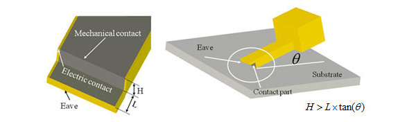
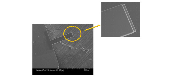
Image of anti-wear probe when drawing patterns