News Releases
Toshiba Starts Construction of Fab 6 and Memory R&D Center at Yokkaichi, Japan
Yokkaichi, Japan—Toshiba Corporation (Tokyo: 6502) today announced that it has started construction of a new state-of-the-art semiconductor fabrication facility, Fab 6, and a new R&D center, the Memory R&D Center, at Yokkaichi Operations in Mie prefecture, Japan, the company’s main memory production base.
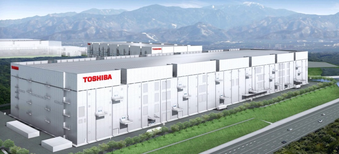
Fab 6 will be dedicated to production of BiCS FLASH™, Toshiba's innovative 3D Flash memory1. Like Fab 5, construction will take place in two phases, allowing the pace of investment to be optimized against market trends, with completion of Phase 1 scheduled for summer 2018. Toshiba will determine installed capacity and output targets and schedules by closely monitoring the market.
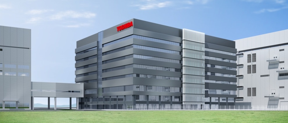
Toshiba will also construct a Memory R&D Center adjacent to the new fab, with completion targeting December 2017. The facility will advance development of BiCS FLASH™ and new memories.
Toshiba is determined to enhance its competitiveness in the memory business by timely expansion of BiCS FLASH™ production in line with market trends, and to retain leadership in innovation in the memory business.
-
Note:
- [1]
- A structure that stacks Flash memory cells on a silicon substrate. It realizes significant density improvements over planar NAND Flash memory, where cells are formed on the substrate. *BiCS FLASH is a trademark of Toshiba Corporation
Artist's impression of Fab 6, Yokkaichi Operations

Artist's impression of Memory R&D Center, Yokkaichi Operations


