News Releases
Toshiba and SanDisk Celebrate the Opening of the Second Phase of Fab 5 and
Start Construction of the New Fab 2 Semiconductor Fabrication Facility at Yokkaichi, Japan


Yokkaichi Operations
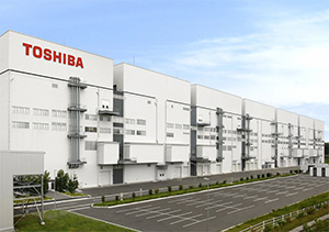
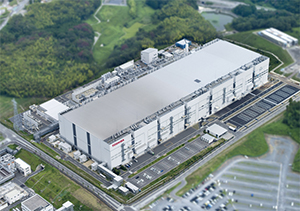
Yokkaichi, Japan, September 9, 2014— Toshiba Corporation (Tokyo: 6502) and SanDisk Corporation (NASDAQ: SNDK) today celebrated the opening of the second phase of the No. 5 semiconductor fabrication facility (Fab 5) and the start of construction of the new No. 2 fabrication facility (Fab 2) at Yokkaichi Operations, Toshiba's NAND Flash memory plant in Mie prefecture, Japan.
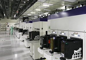
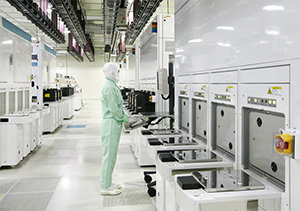
Toshiba started construction of the second phase of Fab 5 in August 2013, and Toshiba and SanDisk have overseen installation of production equipment in the expanded facility since July this year. Production in phase 2 began at the start of this month, with 15nm NAND flash memory process technology, the world's smallest and most advanced node. Toshiba and SanDisk announced deployment of this jointly developed 15nm NAND flash process in April this year, with initial production in part of Fab 5 phase 1, and now target conversion of the remaining capacity in phase 1 to the new process technology.
Toshiba is constructing the New Fab 2 to secure space to convert Toshiba and SanDisk's current 2D NAND capacity to 3D NAND, with expected readiness for production in 2016. Toshiba and SanDisk will together install production equipment and will determine installed capacity and output targets and schedules by closely monitoring market trends.
Yasuo Naruke, Corporate Executive Vice President of Toshiba Corporation and President and CEO of Semiconductor & Storage Products Company, said, "Our determination to develop advanced technologies underlines our commitment to respond to continued demand of NAND flash memory. We are confident that our joint venture with SanDisk will allow us to produce cost competitive next generation memories at Yokkaichi."
Sanjay Mehrotra, President and Chief Executive Officer of SanDisk, said, "We are delighted to further advance the SanDisk/Toshiba collaboration as well as to continue both companies' more than decade- long partnership with the city of Yokkaichi, Mie Prefecture, and Japan. Fab 5 Phase 2 and the future New Fab 2 will provide both companies with the cleanroom space needed to continue converting our installed NAND capacity to new advanced technology nodes."
Toshiba and SanDisk see long-term demand growth for NAND flash memory, particularly for smartphones, tablets and SSDs. The companies will continue to strengthen their competitiveness and market leadership through development and production of advanced flash memory technologies.
Outline of Fab 5 (including phase 2) at Yokkaichi Operations
| Structure of building: | 2-Story steel frame concrete, five floors |
| Building area: | Approximately 38,000m2 |
| Start of construction: | (Phase 1) July 2010; (Phase 2) August 2013 |
| Building completion: | (Phase 1) July 2011; (Phase 2) September 2014 |
Outline of the New Fab 2 at Yokkaichi Operations
| Structure of building: | 2-Story steel frame concrete, five floors |
| Building area: | Approximately 27,300m2 |
About SanDisk
SanDisk Corporation (NASDAQ: SNDK), a Fortune 500 and S&P 500 company, is a global leader in flash storage solutions. For more than 25 years, SanDisk has expanded the possibilities of storage, providing trusted and innovative products that have transformed the electronics industry. Today, SanDisk's quality, state-of-the-art solutions are at the heart of many of the world's largest data centers, and embedded in advanced smart phones, tablets and PCs. SanDisk's consumer products are available at hundreds of thousands of retail stores worldwide. For more information, visit www.sandisk.com.
SanDisk Forward-Looking Statements
This news release contains certain forward-looking statements, including statements about demolition and construction schedules, our timing expectations for first wafer outs, expected production focus at the new clean room, development of new technologies, such as 3D NAND, and products and leadership in NAND memory. There are a number of risks and uncertainties that may cause these forward-looking statements to be inaccurate including, among others: general business and economic conditions; inability to develop, or unexpected difficulties or delays in developing or ramping with acceptable yields, new technologies, such as 3D NAND, or the failure of new technologies to effectively compete with those of our competitors; construction difficulties or delays; our failure to reach definitive agreements with Toshiba on the New Fab 2 or the other risks detailed from time-to-time in our Securities and Exchange Commission filings and reports, including, but not limited to, our most recent quarterly report on Form 10-Q. We do not intend to update the information contained in this release.


