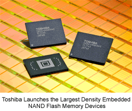
Toshiba Launches the Largest Density Embedded NAND Flash Memory Devices
07 August, 2008
TOKYO--Toshiba Corporation (TOKYO:6502) today announced the launch of 32GB embedded NAND flash memory modules that offer the largest density yet announced plus full compliance with the e-MMCTM(1) and eSDTM(2) standards. The embedded devices are designed for application in mobile digital consumer products, including mobile phones and video cameras. Samples will be available in September 2008, and mass production will start in the fourth quarter. The new 32GB embedded devices combine eight 32Gbit (=4GB) NAND chips fabricated with Toshiba's cutting-edge 43nm process technology and also integrate a dedicated controller. Full compliance with JEDEC/MMCA Ver 4.3 and SDA Ver 2.0, high speed memory standards for memory cards as defined by the MultiMediaCard Association and SD Card Association, respectively, supports standard interfacing and simplified embedding in products, reducing development burdens on product manufacturers. Toshiba offers a line-up of single-package embedded NAND Flash memories which include a controller to manage basic control functions for NAND applications: LBA-NANDTM(3) memory, which has a NAND interface; eSD large capacity chips with SD interface; and e-MMC with an HS-MMC interface. This comprehensive line-up, available in densities ranging from 1GB to 32GB, supports application in a very wide range of products. There is growing demand for memories with a controller function that minimizes development requirements and eases integration into system designs. Toshiba has already taken steps to secure leadership in this expanding market, and the addition of higher density modules will reinforce the company’s position. (1) e-MMC is a trademark of the MultiMediaCard Association
(2) eSD is a trademark of SD Association
(3) LBA-NAND is a trademark of Toshiba Corporation Outline of New Products e-MMC
| Product Number |
Capa. |
Package |
Sample Shipment |
Mass Production |
Production Scale |
| THGBM1G8D8EBAI2 |
32GB |
169Ball FBGA
14x18x1.4mm |
Oct., 08 |
4Q, 08
(Oct.~Dec.) |
1 million/ month
(Total) |
| THGBM1G7D8EBAI0 |
16GB |
169Ball FBGA
12x18x1.4mm |
Sep., 08 |
4Q, 08
(Oct.~Dec.) |
| THGBM1G7D4EBAI2 |
16GB |
169Ball FBGA
14x18x1.4mm |
4Q, 08
(Oct.~Dec.) |
4Q, 08 |
| THGBM1G6D4EBAI4 |
8GB |
169Ball FBGA
12x18x1.3mm |
Sep., 08 |
4Q, 08
(Oct.~Dec.) |
| THGBM1G5D2EBAI7 |
4GB |
169Ball FBGA
12x16x1.3mm |
Oct., 08 |
4Q, 08
(Oct.~Dec.) |
| THGBM1G4D1EBAI7 |
2GB |
169Ball FBGA
12x16x1.3mm |
4Q, 08
(Oct.~Dec.) |
1Q, 09
(Jan.~Mar.) |
| THGBM1G3D1EBAI8 |
1GB |
153Ball FBGA
11.5x13x1.2mm |
4Q, 08
(Oct.~Dec.) |
1Q, 09
(Jan.~Mar.) |
eSD
| Product Number |
Capa. |
Package |
Sample Shipment |
Mass Production |
Production Scale |
| THGVS4G8D8EBAI2 |
32GB |
169Ball FBGA
14x18x1.4mm |
Sep., 08 |
4Q, 08
(Oct.~Dec.) |
500K/ month
(Total) |
| THGVS4G7D8EBAI0 |
16GB |
169Ball FBGA
12x18x1.4mm |
Sep., 08 |
4Q, 08
(Oct.~Dec.) |
| THGVS4G7D4EBAI2 |
16GB |
169Ball FBGA
14x18x1.4mm |
4Q, 08
(Oct.~Dec.) |
4Q, 08 |
| THGVS4G6D4EBAI4 |
8GB |
169Ball FBGA
12x18x1.3mm |
Sep., 08 |
4Q, 08
(Oct.~Dec.) |
| THGVS4G5D2EBAI4 |
4GB |
169Ball FBGA
12x18x1.3mm |
4Q, 08
(Oct.~Dec.) |
4Q, 08
(Oct.~Dec.) |
| THGVS4G4D1EBAI4 |
2GB |
169Ball FBGA
12x18x1.3mm |
4Q, 08
(Oct.~Dec.) |
1Q, 09
(Jan.~Mar.) |
| THGVS4G3D1EBAI8 |
1GB |
153Ball FBGA
11.5x13x1.2mm |
1Q, 09
(Jan.~Mar.) |
1Q, 09
(Jan.~Mar.) |
Key Features
| 1. |
The integrated controller compliant with JEDEC/MMCA Ver 4.3 and SDA Ver 2.0 handles essential functions, including writing block management, error correction (ECC) and driver software. It simplifies system development, allowing manufacturers to minimize development costs and to improve time to market for new and upgraded products. |
| 2. |
A wide product line-up supports capacities from 1 to 32GB. The high-capacity 32GB embedded devices can record up to 560 hours of music at a 128Kbps bit rate, 4 hours of full spec high definition video(4) and 7.3 hours of standard definition video. |
| |
(4) HD and SD are calculated at mean bit rates of 17Mbps and 9Mbps, respectively. |
| 3. |
The 32GB device stacks eight 32Gbit (=4GB) chips fabricated with leading-edge 43nm process technology.
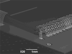
SEM Photograph of 32GB device structure |
|
Specifications e-MMC
| Interface |
JEDEC/MMCA Ver 4.3 standard HS-MMC interface |
| Power Supply Voltage |
2.7 to 3.6V(memory core)/ 1.7V to 1.95V (interface) |
| Bus width |
x1 / x4 / x8 |
| Writing Speed |
Target 10 MB per sec (Sequential Mode)
Target 18 MB per sec (Sequential/Interleave Mode)(5) |
| Reading Speed |
Target 20 MB per sec (Sequential Mode) |
| Temperature |
-25degrees - +85degees Celsius |
| Package |
153Ball FBGA (+16 support Ball) |
(5) Available only for THGBM1G8D8EBAI2 and THGBM1G7D4EBAI2. eSD
| Interface |
SDA Ver 2.0 standard SD interface |
| Power Supply Voltage |
2.7 to 3.6V |
| Bus width |
x1 / x4 |
| Writing Speed |
SDA standard Class 4 |
| Reading Speed |
SDA standard Class 4 |
| Temperature |
-25degrees - +85degees Celsius |
| Package |
153Ball FBGA (+16 support Ball) |
|