
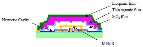
| Toshiba develops cost competitive MEMS packaging technologies 30 May, 2008 --Achieving world's thinnest multi-chip MEMS package with control IC-- TOKYO--Toshiba Corporation today announced two optimized packaging technologies for micro electro-mechanical systems (MEMS) semiconductor packages that achieve significant cost reductions. The first technology covers encapsulation under normal atmospheric condition, the second a stronger structure for vacuum sealing. Both technologies can be applied at the wafer level, and both have been used to achieve multi-chip MEMS packaging with a control IC at a thickness of only 0.8mm, the thinnest yet announced. Both achievements were reported on May 28th and 29th (EST) at the Electronic Components and Technology Conference 2008 held at Florida, U.S.A. from May 28th. As achieving cost efficiency and high productivity is one of the key objectives of MEMS, there are significant demands for small sized, hermetic cavity packaging technologies. Vacuum sealing is utilized in high speed applications, such as MEMS switch and gyroscopes, but there are various problems with this, including ringing. In applications where high speed is not required, such as use in mobile phones, low cost encapsulation under normal atmospheric condition technology is employed. Toshiba has developed both packaging technologies. Toshiba will further develop and optimize these technologies toward establishing for practical use. Feature of development 1. Encapsulation under normal atmospheric condition [Package structure of encapsulation under normal atmospheric condition]
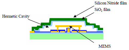
2. Vacuum sealing [Package structure of vacuum sealing]
|
| Information in the news releases, including product prices and specifications, content of services and contact information, is current on the date of the press announcement,but is subject to change without prior notice. |