
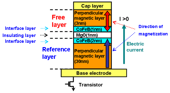
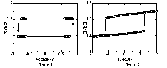
| Toshiba develops new MRAM device which opens the way to giga-bits capacity 06 November, 2007 World's first perpendicular magnetic anisotropy MTJ device Tokyo--Toshiba Corporation today announced important breakthroughs in key technologies for magnetoresistive random access memory (MRAM), a promising, next-generation semiconductor memory device. The company has successfully fabricated a MRAM memory cell integrating the new technologies and verified its stable performance. Full details of the new technologies were presented today at the 52nd Magnetism and Magnetic Materials Conference in Tampa, Florida, USA which is being held from November 5th to 9th. MRAM is a highly anticipated next-generation non-volatile semiconductor memory device that offers fast random write/access speeds, enhances endurance in operation with very low power consumption. MRAM can theoretically achieve high level integration as the memory cell structure is relatively simple. Spin transfer switching uses the properties of electron spin to invert magnetization and writes data at very low power levels. It is widely regarded as a major candidate among next-generation principles for new memory devices. PMA aligns magnetization in the magnetic layer perpendicularly, either upward or downward, rather than horizontally as in in-plane shape anisotropy layers. The technology is being increasingly used to enhance for storage capacity for high-density hard disc drives (HDDs), and Toshiba has successfully applied it to a semiconductor memory device. With PMA data write operation and magnetic switching can be achieved at a low energy level. Toshiba also overcame the hurdle of achieving the required precision in the interface process and significantly cutting write power consumption. In order to realize a miniature memory cell based on PMA, Toshiba optimized the materials and device structure of the new MRAM. Close observation of performance confirms stable operation (see the diagram for full explanation of structure). Toshiba will further enhance development toward establishing fundamental technologies within the coming years. Development of the new MRAM technologies was partly supported by grants from Japan's New Energy and Industrial Technology Development Organization (NEDO). Outline of Development (1) Cell Structure A material with perpendicular magnetic anisotropy, which is used for recording media and a type of cobalt-iron, is employed in the magnetic layer, with magnesium oxide in the insulating layer and cobalt-iron-boron in the interface layers. (2) Operational Results
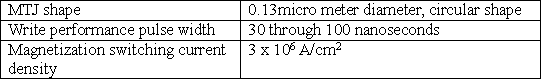
(3) Major characteristics and specifications of MRAM device
|
|||||||||||
| Information in the press releases, including product prices and specifications, content of services and contact information, is current on the date of the press announcement,but is subject to change without prior notice. |