
| Toshiba Completes Construction of Building for 300mm Wafer Fab at Oita Operations in Kyushu 19 February, 2004
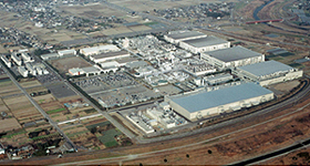
Tokyo -- Toshiba Corporation today announced that it had completed construction of the building for a new 300mm-wafer-fabrication facility at Oita Operations in Kyushu, Japan. The new fab is scheduled to start production in autumn this year, and will mass-produce high-performance System-on-Chip (SoC) LSIs with extremely high levels of integration. A celebratory ceremony held at Oita Operations today marked the successful completion of construction, which began in June 2003. Toshiba will now equip the new facility and its clean room with advanced manufacturing equipment, in readiness for the start of mass production of 300mm wafers in autumn this year. A 200 billion yen investment program from FY2003 to FY2007, will bring production capacity to 12,500 wafers a month. This could be further expanded if necessary, up to a capacity of 17,500 wafers a month, with further investment. Toshiba is reinforcing its leadership in the increasingly important market for the advanced SoC that are at the heart of today's digital consumer products, and the new fab at Oita has a crucial role to play in this strategy. In addition to 300mm wafers, the new fab will draw on Toshiba's industry-leading know-how in embedded DRAM process technology -- essential for high-performance system LSIs -- and will also be the first semiconductor facility in the world to deploy 65-nanometer process and design technologies. In future, Toshiba expects the new fab to lead the industry in introducing 45nm process technology and applying it to SoC devices. Completion of the new Oita facility will place Toshiba in the vanguard of LSI production, enhancing capacity and output and equipping the company to supply the global market with the world's most powerful SoC devices. The new facility at Oita will also support the company in promoting a total solutions business in LSI. Advanced SoC slated for manufacture in the new fab at Oita Operations include wide-ranging system LSIs for digital consumer electronics, mobile products, and broadband network, such as next-generation image processing microprocessor, which demands are expected to increase in the future. The new Oita fab is the first of two advanced 300mm-wafer facilities that Toshiba plans to construct. The second, to be built at Yokkaichi Operations in Mie, Japan, will support the company in meeting fast growing demand for NAND flash memory. These two projects underline Toshiba's determination to retain leadership in the global semiconductor industry, particularly in strategic areas that enhance its ability to deliver to market ahead of its competitors competitive, differentiated semiconductor products based on cutting-edge know-how. Outline of New 300-wafter Facility at Oita Operations
Outline of Oita Operations
|
| Information in the press releases, including product prices and specifications, content of services and contact information, is current on the date of the press announcement,but is subject to change without prior notice. |