
| Toshiba's New Clean Room at Yokkaichi Works Starts Operation State-of-the-Art Facility Can Produce 64Mb and 256Mb DRAMs 30 May, 1996
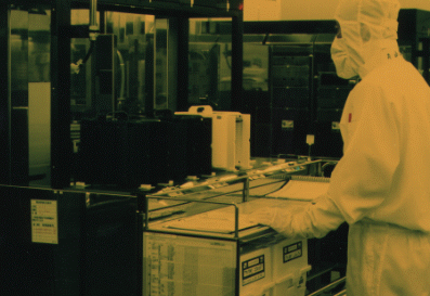
The new facility is designed to undertake all stages of mass production, from wafer fabrication to final assembly and testing. It is equipped with state-of-the-art manufacturing equipment, including support for CMOS processing to the 0.35 micron design rule required for mass production of 64Mb DRAM. It has a total floor area of 60,000 square meters, and attains class-1 air purity -- less than one 0.05 micron in diameter particle in any 1 cubic foot of air. It is equipped for 8- inch size wafers, the largest size currently used in the industry, and has a monthly production capacity of 30,000 wafers. Toshiba's total investment in the clean room's construction and equipment will amount to approximately 100 billion yen under a three-year investment program to March 1997, the end of this fiscal year. The number of employees at Yokkaichi Works has been increased by 600 to 1,600. Initial operations at the new clean room will cover mass production of second- generation 64Mb DRAMs (packaged in a 400-mil (10.2mm) wide package) co- developed with IBM and Siemens, and 16Mb DRAMs. Later projects will include mass production for 256Mb DRAMs, also resulting from the co-development work. The new facility and its manufacturing processes are designed for efficiency -- to output more, faster, with less input of resources. With production in Toshiba semiconductor plants in fiscal 1993 as a reference, the new clean room uses 70% fewer manufacturing processes and the output/input ratio is 40% higher. These gains are the interim results of Toshiba's three-year strategic drive to raise productivity in its semiconductor plants to 2.5 times that at the end of fiscal 1993. In earthquake-prone Japan, another key point of the facility is its earthquake- resistant design. A special floor structure absorbs vibration and prevents it from impacting on manufacturing, thus assuring stable operation. Forecasts of DRAM demand show long term growth in the world market, stimulated by wider use of memory-hungry multimedia equipment. Along with this trend, 64Mb DRAMs are starting to find wider acceptance, and are expected to see annual demand reach 65 million units in 1997. The new clean room will provide Toshiba with a firm basis for meeting current and future demand. It will also serve as a model for the Toshiba-IBM joint venture facility, currently under construction in Manassas, Virginia, due to start manufacturing 64Mb DRAMs from the 4th quarter of 1997. Toshiba is currently producing 16Mb DRAMs at Yokkaichi Work's first clean room, Oita Works and Tohoku Semiconductor Corp., a joint venture in Japan with Motorola Inc. The current monthly production level of 6.5 million 16Mb DRAMs will be raised to 9 million at the end of calendar year 1996, and to 10 million by the end of fiscal 1996.
|
 Outline of Yokkaichi Works
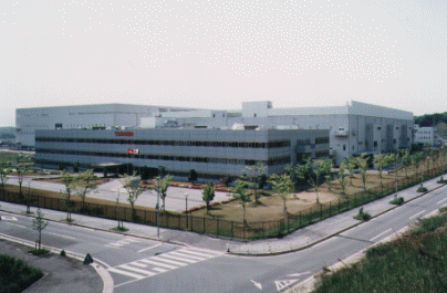
| Information in the press releases, including product prices and specifications, content of services and contact information, is current on the date of the press announcement,but is subject to change without prior notice. |