
| Toshiba Starts Marketing Second Generation 64-megabit DRAMs 23 May, 1996
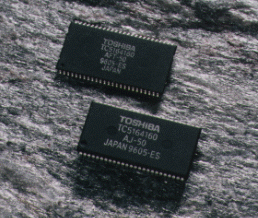
The new TC5164 series is a line-up of leading-edge products offering high speed and low power consumption. Use of EDO (Extended Data Out) allows the devices to achieve an access time of 40 nanoseconds, the world's fastest speed in this class of device, while maintaining power consumption at a low level of 1cc1=100mA operating at around 3.3V. Products are available in a range of multibit-configurations: 16-megaword (M) x 4-bit, 8M x 8-bit and 4M x 16-bit. The 64Mb synchronous DRAM, a derivative of the second generation 64Mb DRAM, is in the final stage of development and is slated for introduction to the market early next year. The products are fabricated utilizing 0.35 micron CMOS processing technology. The new series offers better performance than first generation devices, even while cutting the chip area by around 25 percent, to achieve a size of 167 square millimeters. They are available in 400-mil 32-pin SOJ/TSOP (x4/X8) packages and 50-pin SOJ/TSOP (x16) packages.
 Technological Advantages
Major technologies contributing to chip performance include: Shallow Trench Isolation narrows the gaps between each transistor by utilizing an oxidized isolation wall to assure isolation; Chemical Mechanical Polishing which supports precise processing of the chip by polishing the chip surface before each patterning process. Toshiba, IBM and Siemens began their 256Mb DRAM joint development program at IBM's facility in Fishkill, New York in January 1993. The program was extended to cover development of second generation 64Mb DRAM in mid 1994.
Product Outline
|
| Information in the press releases, including product prices and specifications, content of services and contact information, is current on the date of the press announcement,but is subject to change without prior notice. |