
Overview
TOKYO---Toshiba Corporation has developed a resin-insulated SiC power semiconductor module (SiC power module) that greatly improves power density, which represents the capacity to process power per unit area, by using resin as the insulating substrate through technology for the distributed layout design of small-area chips and design optimization technology using AI, which are unique to Toshiba.
SiC power modules can provide high-capacity power conversion under high voltage and high current, and are becoming widespread in power converters for renewable energy, industry, and electricity-driven transportation such as railroads. Semiconductor modules use an insulating substrate in order to prevent electrical interference with surrounding devices; although resin insulating substrates offer lower cost and longer service life with durability against thermal fatigue (*1), they also have the problems of lower thermal conductivity and higher thermal resistance compared with the ceramic insulating substrates now in widespread use (*2). A large cooling system is needed in order to maintain high performance, but this creates the separate problem of increasing the size of the overall device.
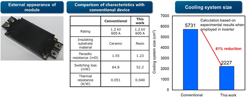
Toshiba has increased the thermal dissipation area and reduced thermal resistance by decreasing the area of chips mounted on a module in comparison with conventional chips and arranging a larger number of chips spread around the entire module. As the number of chips increases, the number of parameters for designing the chip layout also increases and the overall optimal design, including the electrical and thermal characteristics, becomes more difficult. However, an optimal design was possible by means of a unique optimization algorithm using AI (*3). When the distributed layout design of small-area chips and design optimization technology using AI were employed and a prototype resin-insulated SiC power module was tested, it was found to have 21% lower thermal resistance compared with conventional ceramic-insulated SiC power modules. Furthermore, when the developed SiC power modules were used in a general inverter, a trial calculation found that the cooling system size could be reduced by 61%. This technology is expected to enable downsizing of power conversion devices, thereby saving space and reducing costs. This is expected to contribute to achieving carbon neutrality, for example, through further expansion of electric transportation and renewable energy.
Toshiba will present details of this technology at the 37th International Symposium on Power Semiconductor Devices and ICs (ISPSD) 2025, the foremost international conference in the power semiconductor industry, be held in Kumamoto, Japan from June 1 to June 5.
Development background
Power semiconductors, which convert electrical power into an appropriate form (voltage, direct/alternating current, frequency) for efficiently operating equipment, are expected to have increasing market growth in the future against a backdrop of increased electricity generation due to the spread of electric vehicles and renewable energy for achieving carbon neutrality. SiC power modules are equipped with multiple SiC power semiconductor chips capable of high-efficiency power conversion to enable high-capacity power conversion of high voltages and high currents. These modules are becoming widespread in power converters for renewable energy, industry, and electric transportation such as railroads.
The power modules that are currently widely commercialized employ ceramic insulation. Although the Toshiba group also manufactures and sells ceramic-insulated SiC power modules through Toshiba Electronic Devices and Storage Corporation, which is responsible for Toshiba’s semiconductor business, at the same the company has been working on developing resin-insulated SiC power modules that utilize a resin insulating substrate for next-generation devices. Resin-insulated devices are expected to have advantages of lower cost and longer service life with durability against thermal fatigue in comparison with ceramic insulation, but they also suffer from the problems of low thermal conductivity and high thermal resistance. If the thermal resistance is high, it becomes difficult to transport heat through the material, trapping the heat inside. This makes it impossible to effectively dissipate the heat generated by the semiconductor module, causing power loss and consequently causes a decrease in power semiconductor performance including power density.
Power modules generate heat regardless of the type of insulation, including ceramic, meaning that a cooling system is required when incorporating them into power conversion devices in order to remove the generated heat and reduce power losses. Because resin insulating substrates are characterized by poor heat dissipation in comparison with ceramic, a larger cooling system is needed in order to maintain high performance, leading to the further problem that the device becomes large.
Features of the technology
To address the above issues, Toshiba decreased the area of the SiC power semiconductor chips installed in the module, increased the number of mounted chips, and arranged the chips distributed across the entire module. Because the heat dissipation area of the chips is large with a radiance shape toward the heatsink at the bottom of the module, the heat dissipation area increases as the number of chips increases, leading to improved thermal resistance.
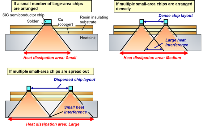
However, if the chips are not arranged appropriately, interference arises between the heat dissipation areas, and the heat dissipation area cannot be enlarged efficiently. Furthermore, as the number of chips increases, the number of module design parameters increases, and it becomes difficult to optimize the overall design taking into account both electrical characteristics such as parasitic resistance (*4) and switching losses (*5) and thermal characteristics. Therefore, a novel AI was used to optimize the module design parameters such as the chip layout and the layout of the copper pattern on which the chips are mounted. As a result, the upper limit of the thermal dissipation area and the number of chips were increased and thermal resistance, parasitic resistance, and switching losses were improved.
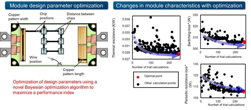
When a prototype of the module structure with the optimized design parameters was created and tested, the prototype resin-insulated SiC power module was found to have 21% lower thermal resistance, 21% lower parasitic resistance, and 19% lower switching loss compared with conventional ceramic-insulated SiC power modules. Although large thermal resistance has been a problem with resin-insulated SiC power modules, the proposed technology not only achieved a large improvement in thermal resistance, but also improved the parasitic resistance and switching losses, and the performance far exceeded that of ceramic-insulated SiC power modules. The reduction effect on the cooling system size when using the developed module in a typical inverter was estimated based on these results, with a trial calculation showing a reduction of 61% in the cooling system size. This technology is expected to enable smaller power conversion devices, leading to space saving and cost reduction. It is also expected to contribute to achieving carbon neutrality, for example, by further increasing the spread of electric transportation and renewable energy.
Future developments
Toshiba aims to conduct further research and development of this technology while also considering the development of power modules with different current and withstand voltage ratings. It also aims to quickly commercialize this technology at Toshiba Electronic Devices and Storage Corporation. Toshiba is working to contribute to achieving carbon neutrality by increasing the performance of various devices for power electronics applications.
- Refers to power cycle durability, which is the reliability of a package when power is applied and the temperature repeatedly rises and then cools in a fixed cycle.
- A value that represents the difficulty of transmitting heat, defined as the temperature rise per applied power.
- Toshiba Corporation developed an AI-based "High-Dimensional Bayesian Optimization Technology" to Automatically Optimize many Parameters that are Difficult to Tune Manually -Promoting digital evolution and transformation in data-driven design of high-performance power semiconductors and other advanced applications- | Corporate Laboratory (Komukai region) | Toshiba
- Refers to tiny resistance components that are unintentionally present in circuits and devices.
- Refers to a loss that occurs when a power semiconductor is switched between on and off.