
- Back to the previous page
- Nano Materials & Devices
Solution-Processed OLED Lighting
Organic light-emitting diodes (OLEDs) are a focus of expectations as a possible new flat-panel light source. Although OLEDs with higher efficiency than fluorescent lights have been reported, they were fabricated by a vacuum evaporation process that is known to be expensive. In order to commercialize OLED lighting, it is necessary to reduce the fabrication cost.
Toshiba focused on solution-processed OLEDs because of their potential for low-cost fabrication without the need for a vacuum apparatus. We employed a substrate with stripe-shaped auxiliary electrodes in order to lower the effective resistance of an indium tin oxide (ITO) anode and reduce the electric potential drop. In addition, we applied a meniscus printing method (shown below), which is a suitable process for uniform coating onto a relief structure.
Consequently, a white OLED panel with a large emitting area of 58 mm × 52 mm and a luminance of 10,000 cd/m2 was obtained, achieving the highest level of luminance for solution-processed OLEDs.
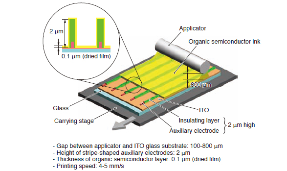
Schematic illustration of meniscus printing method applied to ITO glass
substrate with 2 μm-high stripe-shaped auxiliary electrodes