We live in a world of dramatic change. Companies and societies are trying to tackle increasingly complex issues, and they are turning their attention to quantum technologies. Although it is expected to take some time before we see full-fledged quantum computers that utilize quantum phenomena, Toshiba is already working on quantum-inspired optimization technologies. We are applying our own in-house combinatorial optimization technologies for producing optimal results from massive numbers of options, providing them in the form of the quantum-inspired "SQBM+" optimization solution. This solution uses existing computers to produce highly accurate approximate solutions in short amounts of time. In this running feature, we will explain quantum-inspired optimization technologies.
In Parts 1 to 4 of this running feature, we saw an overview of quantum-inspired optimization technologies and learned about their goals, their position in relation to related technologies, and their applications. We will break the remainder of our coverage on this topic into two parts in which we explain the application of quantum-inspired optimization technologies to real-time or mission-critical systems. In this part, we will talk about FPGAs, which are key devices used to apply this technology. We will also explore what new possibilities can be achieved by combining FPGAs and quantum-inspired optimization technologies.
Important component elements of quantum-inspired optimization technologies and typical classical computers
Quantum-inspired optimization technologies are realized by using existing computers (classical computers) to implement algorithms which were deduced from or whose development was inspired by the logic of quantum computers. Algorithms define sequences of computation or database access.
Therefore, the execution time is not determined by the algorithm alone. Instead, execution times can vary significantly based on what kind of classical computer the algorithm is being implemented in and how well it is being implemented. One of the goals of quantum-inspired optimization technologies is to solve combinatorial optimization problems with speeds impossible to achieve with conventional technologies. Two component elements that are critical for being able to achieve the goals of quantum-inspired optimization technologies are the algorithms that are implemented and the methods used to implement them in computers.
Let's look at the main categories of classical computers used to implement algorithms and compare their features.
The core computer component that is the most familiar to people would surely have to be the CPU (central processing unit). CPUs are responsible not only for controlling overall systems but also running application software as necessary. In many systems, in addition to the CPU (main processor), there are also supplementary components (co-processors). For example, these co-processors perform auxiliary processing to perform certain processes with a shorter response time between input and output than if the CPU were to perform the processing itself (low latency). This auxiliary processing can also increase processing performance per unit of time (high throughput) or reduce power consumption. Because of these uses, co-processors are also called accelerators.
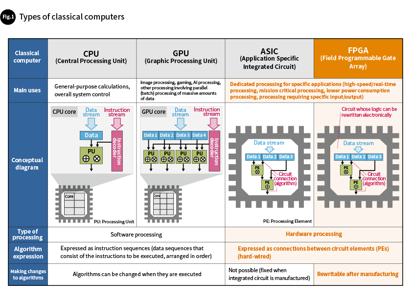
Typical types of co-processors include graphics processing units (GPUs), which are used for image processing, gaming, AI processing, and the like, and application specific integrated circuits (ASICs) and field-programmable gate arrays (FPGAs), which are used for processing that would otherwise cause system bottlenecks or when there is a need for high-efficiency processing, such as in communications or when controlling peripheral devices. ASICs and FPGAs have many characteristics in common, but one big difference between them is whether or not it is possible to rewrite their algorithms once their hardware has been manufactured (Fig. 1).
Different processors have different levels of versatility and processing efficiency
Co-processors are less versatile than CPUs (their range of uses is more limited), but their processing is more efficient.
For each of their processing cores, CPUs have a powerful processing unit (PU). PUs can perform basic processing such as addition, multiplication, shifting, data loading, and data storing, and can also be used to perform more advanced extended processing. Of these, a single process is performed each clock cycle (the unit of processing time of a digital circuit). Executed processes are ordered by an instruction decoder. When this happens, the algorithm expresses the instructions to be executed as data sequences (sequences of instructions) arranged in order.
GPUs excel at efficiently executing relatively simple processes on massive amounts of data. GPU cores have many simple PUs, and all of these PUs share a single instruction decoder. This hardware structure is capable of efficiently processing multiple items of data at the same time.
These CPUs and GPUs perform software processing. The next components we will look at, ASICs and FPGAs, differ significantly in that they perform hardware processing. In software processing, algorithms are expressed as sequences of instructions. In the case of hardware processing, on the other hand, algorithms are expressed as connections between circuit elements (called hard-wired algorithms).
For example, let's examine an ASIC or FPGA-implemented algorithm that multiplies Data 1 by Data 2 and then adds Data 3 to the resulting number. As the overview diagram in Fig. 1 shows, this algorithm is expressed as a connection between the outputs of Data 1 and Data 2 and the input of the multiplication processing element (PE), and a connection between the outputs of the multiplication processing element and Data 3 and the input of the additive processing element (PE). A circuit that expresses a certain algorithm is called a dedicated circuit or dedicated hardware. When digital signals for Data 1 to Data 3 pass through the dedicated hardware shown in Fig. 1, hardware processing produces the data of the algorithm's results.
In general, hardware processing is faster and more efficient than software processing. For example, let's consider an algorithm that can simultaneously perform 1,000 multiplication operations. In hardware processing, it is possible that 1,000 multiplication PEs are used, and all multiplication operations are completed within a single clock cycle. When running this same algorithm on a CPU with a single PU (software processing), this will require a minimum of 1,000 clock cycles.
How FPGAs work and how their applications differ from those of ASICs
ASICs and FPGAs are both semiconductor integrated circuits in which hardware designers design dedicated hardware for individual algorithms. In the case of ASICs, dedicated hardware is physically manufactured in a semiconductor production plant. Their algorithms cannot be rewritten after they are manufactured. FPGAs, on the other hand, are information processing circuits that can be electrically rewritten after they are manufactured (Fig. 2).
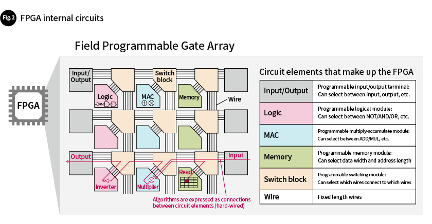
FPGAs contain ordered rows of circuit elements (programmable circuit elements) whose functions can be changed by electrically switching their connections. Programmable circuit elements include input/output terminals, logic modules, multiply-accumulate modules, memory modules, switching modules, and more. These can be used to create the dedicated hardware as desired. Fig. 2 shows an example of dedicated hardware in red-colored lines. The dedicated hardware shown in the figure multiplies data input via the input terminal and data stored in memory (MUL operation), inverts the result (NOT operation), and then outputs the result from one of the hardware's terminals.
Since FPGAs can be rewritten after they are manufactured, the process from deciding on an algorithm to deploying the product takes less time than it would with an ASIC. Furthermore, there is no need for development cost for an actual chip (no non-incurring cost). However, the chip sizes of FPGAs are larger than those of ASICs that provide the exact same hardware functions (i.e., the unit cost per chip is higher). This is because FPGAs must contain complex circuit structures to enable their rewritability, and this gives them a larger area. Due to these characteristics, ASICs tend to be used for mass-production products which require a high level of processing efficiency, while FPGAs are used in small-volume products which require short development times.
Quantum-inspired optimization technologies achieved through implementation on FPGAs, which have exceptional levels of processing efficiency
The Simulated Bifurcation Algorithm (SB Algorithm) is a quantum-inspired algorithm which was derived from Toshiba's "quantum bifurcation machine," a quantum computer. In Parts 1 and 2 of this special feature, we discussed how its new mechanisms find good solutions out of massive numbers of options. The key feature of the SB Algorithm, from a classical computer implementation perspective, is its high level of parallelism (the number of calculations that can be performed in the same clock cycle).
The co-processors we have discussed above all use parallel processing to achieve a higher level of processing efficiency than a CPU, but that does not mean that they can execute all algorithms with a high level of efficiency. In addition to algorithms having a high degree of parallelism, their structure (data dependency) must also have a high level of affinity with the architecture of classical computers. One of the features of the SB Algorithm is that it has a high level of affinity with not only GPU architecture but also FPGA architecture.
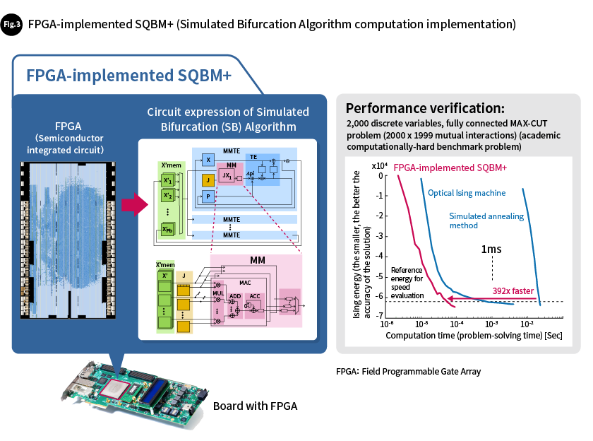
The first example of implementing the SB Algorithm on an FPGA was presented in a paper published in 2019 (https://doi.org/10.1126/sciadv.aav2372). In this case, dedicated, massively parallel hardware was designed to fully leverage the parallelism of the SB Algorithm, and it was implemented using a single FPGA. There were 8,192 multiply-accumulate modules, and this massive number of multiply-accumulate modules performed effective calculations in 92% of clock cycles. This shows that hardware with a high level of spatial parallelism also has a high degree of temporal activity (with short idling times).
For an academic benchmark problem that is proven to be difficult to solve (a combinatorial optimization problem), this implementation was found to be 392 times faster than using the simulated annealing algorithm, a conventional classical algorithm, while producing an equivalent quality of solution (a solution with an equivalent level of Ising energy) (Fig. 3).
Providing greater value by combining quantum-inspired optimization technologies and FPGAs
The SB Algorithm, a quantum-inspired algorithm, can be implemented with a high level of efficiency on GPUs and FPGAs. This high efficiency implementation refers to using numerous circuit resources in a classical computer without wasting any of them, and activating those circuit resources to perform computation effectively, without any idling times.
The SB Algorithms implemented using GPUs and FPGAs both have high levels of processing efficiency, but they have different characteristics that reflect the differences between the architecture of the two co-processors (Fig. 4).
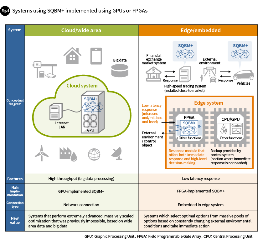
One of the features of GPU implementation is its high throughput. This assists with the creation of systems for solving massive combinatorial optimization problems or high numbers of problems. The GPU resources in cloud computing environments can be used to develop systems capable of performing extremely advanced, massive optimization, based on wide-ranging data and big data, that have been impossible with conventional systems.
FPGA implementation, on the other hand, offers the benefit of low-latency response. It can be used when building edge systems that select optimal options from massive numbers of options depending on constantly changing external environmental conditions and take immediate action. This low-latency response is made possible by integrating not only dedicated quantum-inspired algorithm hardware but also other system modules into a single FPGA. Some of the potential fields in which these FPGA-implemented SQBM+ quantum-inspired optimization solutions can be applied include advanced high-speed financial trading systems and vehicle-mounted control systems.
In this issue, we have learned about what FPGAs are and the features of quantum-inspired optimization technologies implemented using FPGAs. In Part 6, we will look at specific examples of financial and vehicle-mounted systems that use FPGAs with SB Algorithms. Don't miss it.
TATSUMURA Kosuke
Fellow, Computer & Network Systems Laboratory, Information & Communication Platform Laboratories, Corporate Research & Development Center, Toshiba Corporation
Fellow, New Business Development Group, Data Business Promotion Dept., ICT Solutions Division, Toshiba Digital Solutions Corporation
Since joining Toshiba, TATSUMURA Kosuke has been engaged in R&D regarding domain-specific computing. He is currently conducting R&D and business development related to the quantum-inspired optimization solution SQBM+.
YAMASAKI Masaya
Expert, Computer & Network Systems Laboratory, Information & Communication Platform Laboratories, Corporate Research & Development Center, Toshiba Corporation
After joining Toshiba, YAMASAKI Masaya designed and developed circuits for increasing the edge quality of TV images and implemented FPGA high speed circuitry using high-level design. He is currently engaged in R&D related to the quantum-inspired optimization solution SQBM+.
- The corporate names, organization names, job titles and other names and titles appearing in this article are those as of March 2025.
- SQBM+ is a registered trademark or trademark of Toshiba Digital Solutions Corporation in Japan and other countries.
- All other company names or product names mentioned in this article may be trademarks or registered trademarks of their respective companies.
>> Related information
Related articles
Running Feature: Quantum-inspired optimization technologies that rapidly produce optimal solutions from massive, complex sets of options(Article list)