2014年 研究開発センター パンフレット
概要
シリコンに替わるワイドバンドギャップ材料SiC(炭化珪素)、GaN(窒化ガリウム)を利用し、パワー半導体デバイスの電力損失を大幅に低減します。インバータや電源の小型化・高効率化を加速し、情報機器電源、ハイブリッド車や太陽光発電などのエネルギー効率向上を目指します。
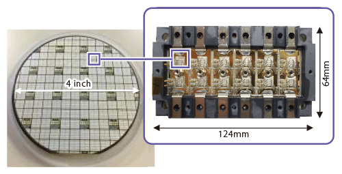
SiC-MOSFETチップ※を適用した1.7kV 360Aモジュール
※NEDO(独立行政法人 新エネルギー・産業技術総合開発機構)、「戦略的省エネルギー技術革新プログラム」の助成を受けて開発。
関連情報
- 2015. 05 [国際会議発表]
- K. Takao and S. Kyogoku, “Ultra Low Inductance Power Module for Fast Switching SiC Power Devices,” in Proc. ISPSD2015, pp. 313-316.
- 2014. 06 [国際会議発表]
- H. Kono, et al., “High-speed and Low Switching Loss Operation of 1700V 60A SiC MOSFETs Installed in Low Parasitic Inductance Module,” in Proc. ISPSD2014, pp. 289-292.
- 2014. 03 [国際会議発表]
- K. Takao, et al., “1200 V-360 A SiC Power Module with Phase Leg Clustering Concept for Low Parasitic Inductance and High Speed Switching,” in Proc. CIPS 2014, pp. 482-488
- 2013.09 [国際会議発表]
- H. Kono, et al., "14.7mΩcm2 3.3 kV DIMOSFET on 4H-SiC(000-1)", ICSCRM 2013, Tu-P-55.
- 2013.09 [国際会議発表]
- K. Ariyoshi, et al., "Nitridation effects of gate oxide on channel properties of SiC trench MOSFETs", ICSCRM 2013, We-3A-5.
- 2013.09 [国際会議発表]
- C. Ota, et al., "VF Degradation of 4H-SiC PiN Diode Using Low-BPD Wafers", ICSCRM 2013, Th-P-34.
- 2013.03 [論文]
- H. Saito et al., "Over 550 V breakdown voltage of InAlN/GaN HEMT on Si", Physica Status Solidi (c), Vol. 10, 5, 824 (2013).
- 2013.02 [論文]
- K. Takao and H. Ohashi: Accurate Power Circuit Loss Estimation Method for Power Converters With Si-IGBT and SiC-Diode Hybrid Pair, IEEE Trans. on Electron Devices, Vol. 60, No. 2, 606-612 (2013)
- 2012.06 [東芝レビュー]
- 低接触抵抗オーミック電極によるKa帯GaN HEMT特性の改善(298KB/PDFデータ)
