Technology
Toshiba Announces Gallium Nitride Power FET With World's Highest Power Output
Achievement of 174W output power at 6GHz will support enhanced microwave communications
Tokyo-Toshiba Corporation today announced development of a gallium nitride (GaN) power field effect transistor (FET) that far surpasses the operating performance of the gallium arsenide (GaAs) FET widely used in base stations for terrestrial and satellite microwave communications. The new transistor achieves output power of 174W at 6GHz, the highest level of performance yet reported at this frequency.
Toshiba realized this breakthrough performance enhancement by optimizing the epitaxial layer and chip structures for 6GHz-band operation and by adopting a four-chip combination structure to minimize heat build-up. The result is a GaN power FET with eight times the power density of a GaAs FET and the worldRs highest output power at the 6GHz frequency level.
Having proven the design concept, Toshiba will continue to refine the technology, toward the target of sample releases next year. The new FET is expected to become a key component in microwave communications.
Full details of the new GaN power FET and its technology will be presented at the International Conference on Solid State Devices and Materials (SSDM), from September 12 to 15 in Kobe, Japan.
Background and development aims
Ever increasing communications flows are driving demand x? for higher output power in the amplifying devices used in base stations for terrestrial and satellite microwave communications. Until now, Toshiba has met this demand with GaAs-based FETs offering 90W output power at 6GHz frequency and 30W at 14GHz.
However, heat dissipation is a critical issue with GaAs, to the point that the material is fast approaching the upper limits of its performance characteristics.
GaN shows great promise for application in amplifiers that support higher frequencies than the microwave band, since it offers higher saturation electron velocity, higher dielectric breakdown voltage and a higher operating temperature range than GaAs. Toshiba has focused on development of materials that can operate at a higher frequency than the C-band (4GHzi8GHz) and succeeded in demonstrating the worldRs highest power output by a GaN power FET at 6GHz by structural optimization of the device. Toshiba is confident that it can achieve even higher output levels as it continues its development activities.
New technologies
- 1 Epitaxial layer structure
The power FETs adopts a High Electron Mobility Transistor (HEMT) structure. By optimizing conditions of doping and the thickness of the AlGaN and GaN layers, Toshiba achieved outstanding performance.
- 2 Chip structure
Working with the new epitaxial layer structure, Toshiba processed and optimized the FET unit structure, including gate length and distance of source and drain electrodes and this produced high performance in the C-band and higher frequencies.
Fig. 1
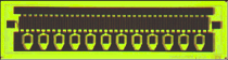
Photograph of GaN power FET chip
* Chip size: 2.92mm×0.71mm - 3 Process and package
Toshiba's newly developed surface treatment process and heat treatment technology achieve low contact resistance at the source and drain electrodes, allowing maximization of the GaN material characteristics. A unique gate electrode structure contributes to cut gate leakage current to 1/30 that of the conventional technology.
Fig. 2
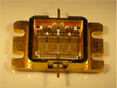
Photograph of packaged device with four chips
* cavity size(outer):
24.5mm×17.4mm - 4 Stepper lithography
While electron beam exposure technology has been commonly used in a lithography process for GaN power FET in the C band and higher frequencies, Toshiba has adopted stepper exposure that is better suited to mass production.
September 12, 2005